4) ROM SPACE
Fig.5 shows the ROM space. The UP-600 uses 2MB of NOR-type
flash memory instead of conventional ROM, so that the FROS1# from
the MPCA9 is input into the chip enable of the flash memory.
5) VRAM & RAM SPACE
The VRAM is the display memory of the LCD.
6) EXTENDED I/O AREA
The addresses from F00000h to FFFFFFh are called an extended I/O
area. The UP-600 uses the following addresses as the break address
register (BAR) for SSP.
• FFFF00h ∼ FFFFFFh
4. LCD DISPLAY
The UP-600 uses a 320 x 240 dot monochromatic LCD for the main
display and VGAC (M66271) for the display controller which is con-
nected to H8/510 in the ISA bus connection mode.
1) BLOCK DIAGRAM
Here is the block diagram of the LCD and its allied components.
2) LCD PANEL
The LCD panel uses a dot-matrix liquid crystal module with mono-
chromatic STN and CCFT backlight. The resolution is 320 x 240.
3) DISPLAY CONTROLLER
Matsushita VGAC (M66271) is used for the display controller.
VRAM is present on the address space of the CPU and it is possible
to write and read data from the CPU side through the lower 9600 byte
address of 128 KB size in addresses C00000H ~ C1FFFFH.
C00000H - C1FFFH:
4) LCD ON CONTROL
The LCD is turned on and off by controlling the bias power supply for
the LCD using the terminal LCDENB of the M66271.
LCDENB is in low level when resetting. When bit 0 of the mode
resistor of the M66271 by software is set to high level, the power is
supplied to the LCD, thus turning on the LCD.
5) BACK LIGHT CONTROL
The backlight ON/OFF is controlled by the same LCDENB used for
controlling the LCD ON mode.
6) LUMINANCE AND CONTRAST ADJUSTMENT
•
Luminance: Luminance is adjusted with an inverter which controls
the dimming function. (Fixed)
• Contrast: Contrast is adjusted by controlling the contrast adjust-
ment voltage (VO) of the LCD.
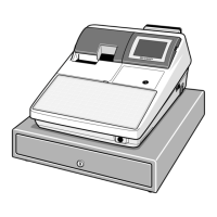
5. CUSTOMER DISPLAY
The UP-600 can incorporate a UP-P16DP for the customer display.
6. SRAM (Standard)
The device is HYUNDAI 4MB SRAM (HY628400ALLT2-70 512K 8bit)
with an access time of 70ns.
200000h
(MAX4MB)
ROS1
5FFFFF
* Lower 64KB of the ROS1 is
mapped on the 0 page area.
* ROS1 is decoded by
MPCA9.
600000h
C00000h
800000h
A00000h
CFFFFFh
RASPN1
VRAM
(2MB)
RASPN2
(4MB)
(1MB)
* All the decode signals in the
area in the figure are supported
by MPCA9.
* RAS1 signals from MPCA9
correspond to 2MB 600000h to
7FFFFFh.
* OPTION RAM board (2MB and
4MB) interfaces using RAS2
as the base signal.
* The actual VRAM is 128KB,
but it is accessed by every
128KB of bank according to
VGAC specification.
CPU
H8/510 SD0-7
A0-13
RD#
RD#
HWR#
LWR#
PHAI CLK
WAIT#
UD0-3 LD0-3
WAIT#
LCD (320 x 240)
MPCA8
LP LP
LCDWT
FLM FP
VIO# IOCS#
DCLK DCLK
VMEM# MCS#
VEE BACKLIGHT
M66271
MBIAS
POWER
LCDENB
8bitMPU connection setting
HWR# : "H"
BHE# : "H"
MPUSEL : "L"