28
A30808-X3247-L14-2-7618
Technical Description (TED:BSS)
BS-240/241
Information
Base Station System
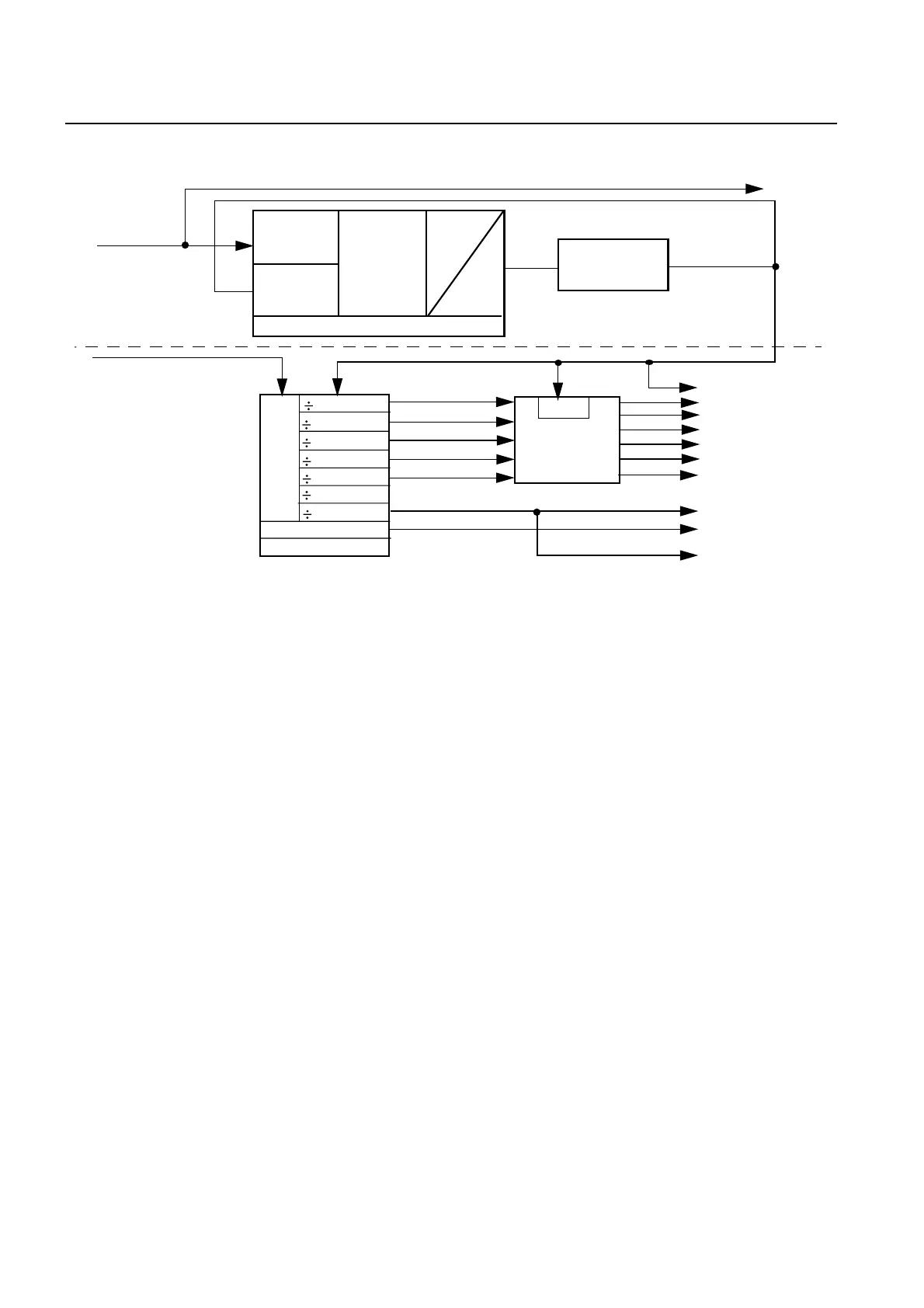
Fig. 3.3 Structure of ACLK Function
The tracking oscillator TOP synchronizes the oven controlled VCXO to the selected
frequency reference source. The TOP is realized as a phase/frequency locked loop. The
regulation parameters (P and I constant) are variable by SW. Also, the regulating algo-
rithm is implemented by SW. The output clock of the oscillator is called the master clock.
The cut-off frequency of the TOP depends directly on the pulling gradient of the used
OCVCXO. Since the ACLK has to synchronize to jittered lines the scattering of the
cut-off frequency is very critical. The cut-off frequency has to choose very low to elimi-
nate lowest frequency wander and is therefore near the range of the temperature’s
cut-off frequency. To guarantee less deviation of the required cut-off frequency also with
components from different manufactures (2nd and 3rd source), the OCVCXO is cali-
brated on the COBA in the factory. The pulling gradient is measured against an atomic
clock and the calibration values is stored on COBA in a serial EEPROM. With Uncali-
brated ACLKs must not be installed in the field. This can be achieved by the software
which should check whether the ACLK is calibrated or not.
In case of redundancy switch-overs no warm up and only a short synchronization phase
(because of effects at the switch-over) of the redundant ACLK is necessary.
The loadable timing generation hardware LTG is implemented in a FPGA device, which
can be loaded by the BCC with the current hardware function. In this stage, all neces-
sary system clocks and the master sync pulse are generated. Also, the master counter
is realized. The count value of the master counter is fed via a serial interface to the
SELIC. In active redundancy mode, the master sync pulse is forwarded to the standby
ACLK. In standby redundancy mode, the generator is synchronized with the master
sync pulse coming from the active ACLK function. So both redundant ACLKs generate
their clocks in aligned. If necessary, a very fast redundancy switch-over is possible.
The FPGA is configured after a power-on reset from the BCC. Until the configuration has
finished, no output clocks are available, i.e., a communication via Abis or CUs is not
reference
clock
divider
master
clock
divider
phase/
frequency
detector
D
A
BCC interface
OCVCXO
32, 768 MHz
master clock
reference
clock input
TOP
tracking
oscillator
processor
controlled
master sync input
from redundant ACLK
LTG
loadable
timing
generator
2
4
8
16
4096
1966080
master counter
BCC Interface
S
Y
N
C
16,384 MHz
8,192 MHz
4,096 MHz
2,048 MHz
8 kHz
60 ms
SYNC
Driver
Stage
system
clocks
master sync
master counts
master sync to redundant ACLK
reference clock to redundant ACLK
 Loading...