5.
Appendix
5.1
Pin assignments
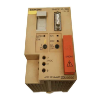
S5-010
bus signal assignments
Socket connectors
B0
.. .
B4
Addressing of blocks
KO..
.
K2
Addressing of inputs and outputs in the selected block 2 1
FP
Enabling of I10 module outputs
DIN Signal status of inputs 4 3
D,, Signal status for setting the outputs
RI Initializing pulse
IR Interrupt request, group interrupt signal of relevant input/
6 5
timer module
M
0
V
DC
(GND)
8
7
The pin numbers are marked on the socket connectors.
Front connector pin assignments
The identification of the pins and their geometrical arrangement are shown in Fig. 30.
The correlation between connector pins and
inputloutput addresses (without coding jumpers) is shown in the following tables.
Input/timer module 6ES5400-OAA11 Digital output module 6ES54104AA41
Pin
2
4
6
8
10
12
14
16
18
20
22
24
26
28
30
32
Pin d b
z
Q0
Q 1
Q2
Q3
Q4
Q5
Q6
16
17 Q7
b
102.0
102.1
102.2
102.3
102.4
102.5
102.6
102.7
M
-
-
-
-
-
-
M
d
101.0
101.1
101.2
101.3
101.4
101.5
101.6
181.7
104.0
104.1
104.2
104.3
104.4
104.5
104.6
104.7
zbd
2
103.0
103.1
103.2
103.3
103.4
103.5
103.6
103.7
,
105.0
lffi.
l
1ffi.2
16.3
1'23.4
16.5
IE.6
Iffi.7
Fig.
30
Front connector pin
assignments (looking
at plug connector)
Digital output module 6ES5410-OAA12
1
Interface module 6ES5 7724AA12
OAA22
 Loading...