Si5338-RM
4 Skyworks Solutions, Inc. • Phone [781] 376-3000 • Fax [781] 376-3100 • sales@skyworksinc.com • www.skyworksinc.com
Rev. 1.4 • Skyworks Proprietary Information • Products and Product Information are Subject to Change Without Notice • 2021
1. Introduction
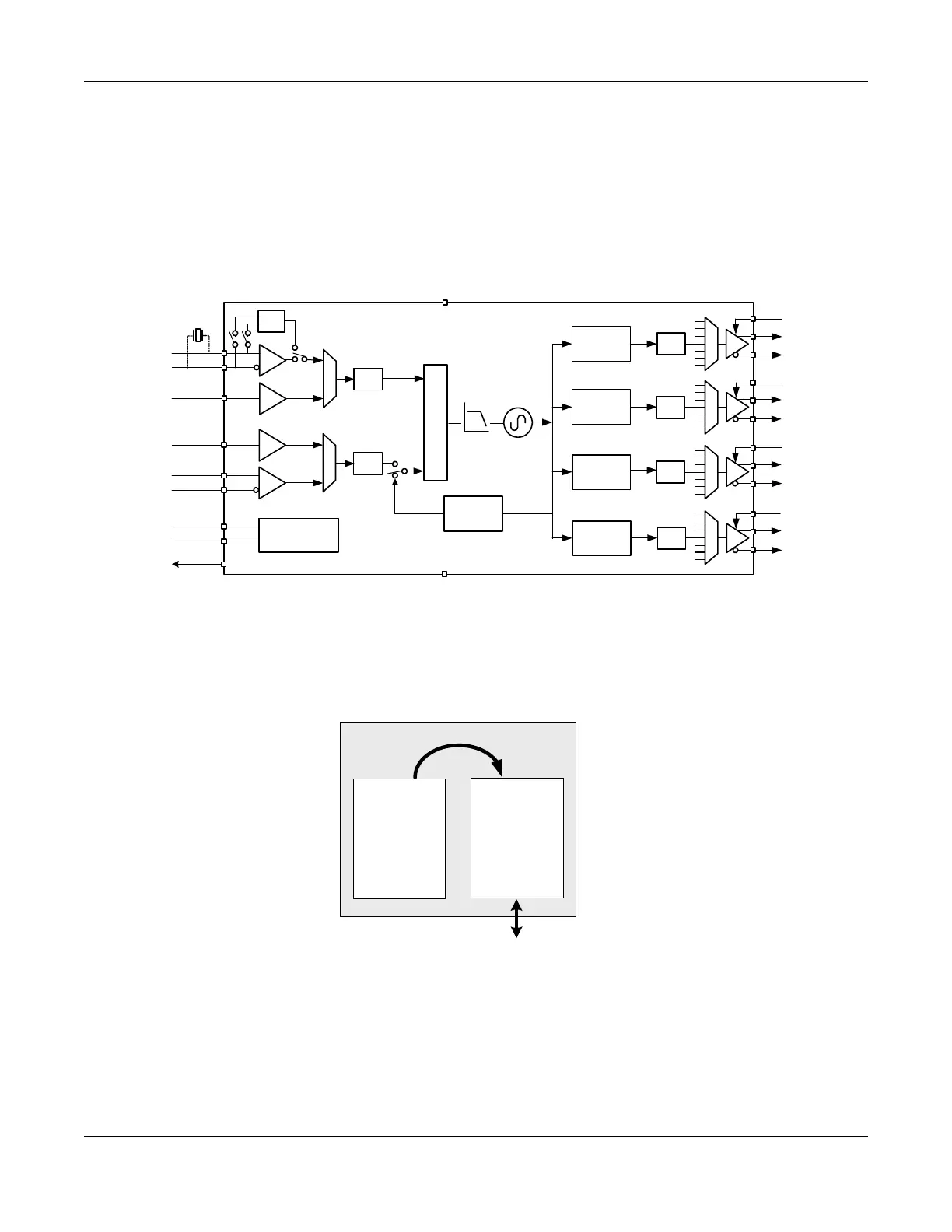
The Si5338 is a highly flexible and configurable clock generator/buffer. A block diagram of the Si5338
programmable clock IC is shown in Figure 1.
To support the flexibility, Skyworks Solutions has created ClockBuilder Pro to create register maps automatically
and easily for a given configuration. Since programming with ClockBuilder Pro may not always be well suited to
every system's requirements, this document presents the procedures and equations for determining a complete
register set from a frequency plan.
Figure 1. Si5338 Block Diagram
The device may have a factory defined default configuration stored in non-volatile memory (NVM). During
powerup, the default configuration is copied into random access memory (RAM). Having its working configuration
stored in RAM allows in-system configuration changes through the I
2
C port. The memory configuration of the
Si5338 is shown in Figure 2.
Figure 2. Si5338 Memory Configuration
This application note provides details on configuring the Si5338 by accessing its RAM space through the I
2
C bus.
CLK0A
÷R
0
÷R
2
MultiSynth
÷MS3
÷R
3
VDDO1
VDDO2
VDDO3
VDDO0
MultiSynth
÷MS2
MultiSynth
÷MS1
MultiSynth
÷MS0
CLK0B
CLK1A
CLK1B
CLK2A
CLK2B
CLK3A
CLK3B
÷P
1
IN3
IN2
IN1
Osc
PD
3
2
1
20
22
21
Si5338
16
18
17
15
14
13
11
10
9
V
DD
7, 24
Optional
XTAL
÷P
2
IN4
IN6
IN5
4
6
5
19
12
SDA
SCL
I
2
C Control
GND
23
INTR/
LOS/LOL
8
Ext
Int
VCO
LPF
MultiSynth
÷N
÷R
1
Power-Up
I
2
C
Si5338
NVM
Default
Configuration
RAM
Working
Configuration