TAS5707
www.ti.com
................................................................................................................................................. SLOS556A – NOVEMBER 2008 –REVISED APRIL 2009
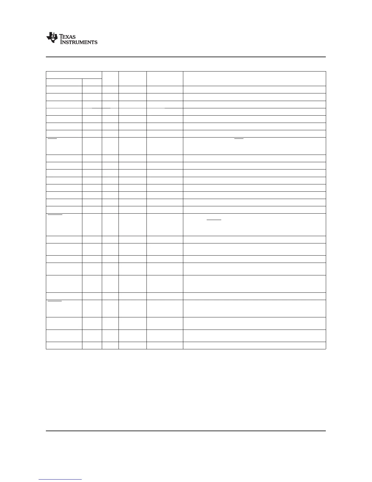
PIN FUNCTIONS (continued)
PIN
TYPE 5-V TERMINATION
DESCRIPTION
(1)
TOLERANT
(2)
NAME NO.
NC 8 – No connection
OC_ADJ 7 AO Analog overcurrent programming. Requires resistor to ground.
OSC_RES 16 AO Oscillator trim resistor. Connect an 18.2-k 1% resistor to DVSSO.
OUT_A 1 O Output, half-bridge A
OUT_B 46 O Output, half-bridge B
OUT_C 39 O Output, half-bridge C
OUT_D 36 O Output, half-bridge D
PDN
19 DI 5-V Pullup Power down, active-low. PDN prepares the device for loss of power
supplies by shutting down the noise shaper and initiating PWM stop
sequence.
PGND_AB 47, 48 P Power ground for half-bridges A and B
PGND_CD 37, 38 P Power ground for half-bridges C and D
PLL_FLTM 10 AO PLL negative loop filter terminal
PLL_FLTP 11 AO PLL positive loop filter terminal
PVDD_A 2, 3 P Power supply input for half-bridge output A
PVDD_B 44, 45 P Power supply input for half-bridge output B
PVDD_C 40, 41 P Power supply input for half-bridge output C
PVDD_D 34, 35 P Power supply input for half-bridge output D
RESET
25 DI 5-V Pullup Reset, active-low. A system reset is generated by applying a logic low
to this pin. RESET is an asynchronous control signal that restores the
DAP to its default conditions, and places the PWM in the hard mute
state (tristated).
SCL 24 DI 5-V I
2
C serial control clock input
SCLK 21 DI 5-V Pulldown Serial audio data clock (shift clock). SCLK is the serial audio port input
data bit clock.
SDA 23 DIO 5-V I
2
C serial control data interface input/output
SDIN 22 DI 5-V Pulldown Serial audio data input. SDIN supports three discrete (stereo) data
formats.
SSTIMER 6 AI Controls ramp time of OUT_X to minimize pop. Leave this pin floating
for BD mode. Requires capacitor of 2.2 nF to GND in AD mode. The
capacitor determines the ramp time.
STEST 26 DI Factory test pin. Connect directly to DVSS.
FAULT
14 DO Backend error indicator. Asserted LOW for over temperature, over
current, over voltage, and under voltage error conditions. De-asserted
upon recovery from error condition.
VR_ANA 12 P Internally regulated 1.8-V analog supply voltage. This pin must not be
used to power external devices.
VR_DIG 18 P Internally regulated 1.8-V digital supply voltage. This pin must not be
used to power external devices.
VREG 31 P Digital regulator output. Not to be used for powering external circuitry.
Copyright © 2008–2009, Texas Instruments Incorporated Submit Documentation Feedback 7
Product Folder Link(s): TAS5707