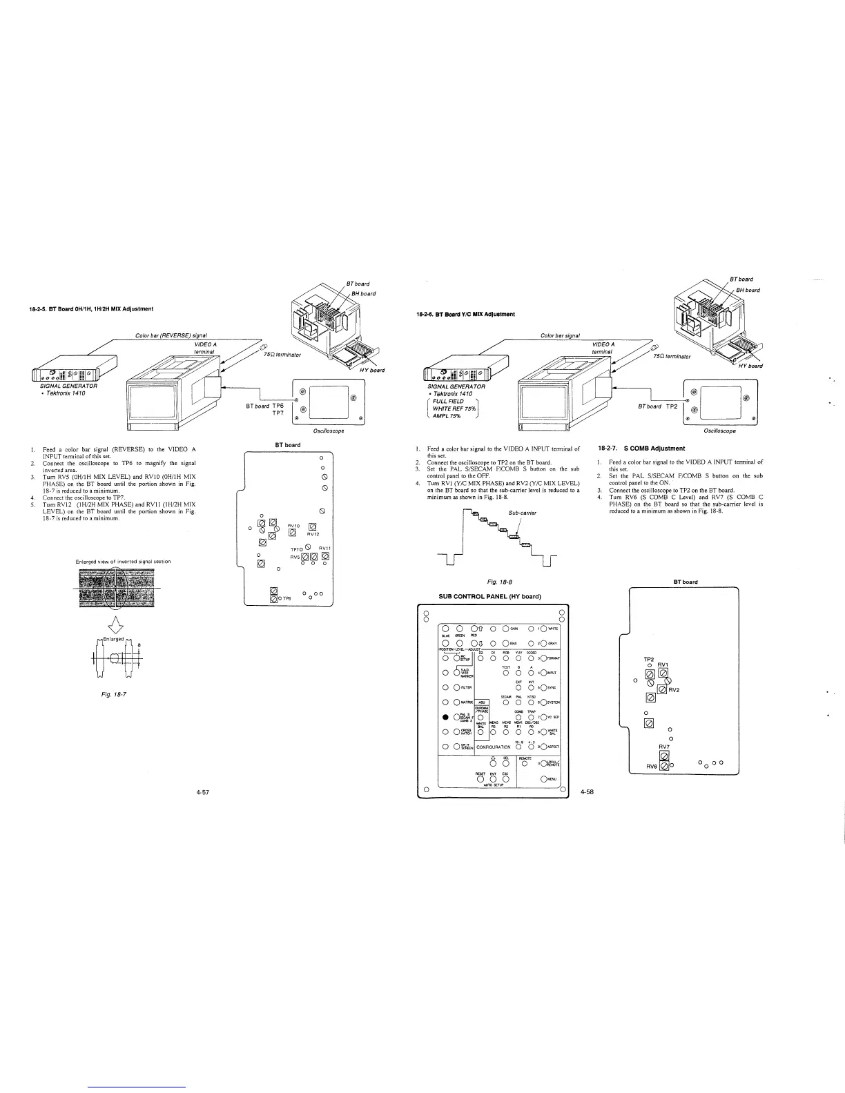
18-2-5. BT Board 0H/1H, 1H/2H MIX Adjustment
1.
2.
3.
4.
5.
Color bar (REVERSE) signal
VIDEO A
terminal
SIGNAL GENERATOR
• Tektronix 1410
Feed a color bar signal (REVERSE) to the VIDEO A
INPUT terminal of this set.
Connect the oscilloscope to TP6 to magnify the signal
inverted area.
Tum RVS (0H/lH MIX LEVEL) and RVJO (0H/lH MIX
PHASE) on the BT board until the portion shown in Fig.
18-7 is reduced to a minimum.
Connect the oscilloscope to TP7.
Tum RV12 (1H/2H MIX PHASE) and RVJ 1 (1H/2H MIX
LEVEL) on the BT board until the portion shown in Fig.
18-7 is reduced to a minimum.
Enlarged view of inverted signal section
0
Enlarged
a
Fig. 18-7
4-57
BT board TP6
TP7
·®D®
®
@ @
Oscilloscope
BT board
0
~
0
RV10
~
~
RV12
0
0
0
0
TP700 RV11
RVS~~~
0 0 0
18-2-6. BT Board Y/C MIX Adjustment
I.
2.
3.
4.
SIGNAL GENERATOR
• Tektronix 1410
[
FULL FIELD J
WHITE REF 75%
AMPL 75%
Color bar signal
Feed a color bar signal to the VIDEO A INPUT terminal of
this set.
Connect the oscilloscope to TP2 on the BT board.
Set the PAL S/SECAM F/COMB S button on the sub
control panel to the OFF.
Tum RV! (Y/C MIX PHASE) and RV2 (Y/C MIX LEVEL)
on the BT board so that the sub-carrier level is reduced to a
minimum as shown in Fig. 18-8.
Sub-carrier
Fig. 18-8
~
~0TP6
0 00
o SUB CONTROL PANEL (HY board)
0 0
0 0
0 0
Oil 0
OGAJN
0
1Q'Nt-1tTE
BLUE
GREEN
RED
0 0
Qij
0
Qa1AS
0
2Q GRAY
POSITION -LEVEL-ADJUST
~o
Dl
RGB YlN
CODED
0 0
0
0
3QFORMAT
TEST
B
A
0 ~g-
0
0
0
401NPUT
MARKER
EXT INT
0
0 FILTER
0 0
sQsYNC
SECAM PAL NTSC
0
OMATAIX
ASU
0 0
o sQsYSTEM
,___
CHROMA
/PHASE
CCMB TRAP
•
o;twi F
0
0
0 1QYc SEP
CCMB S
MEM3
MEM2 MEM1 D65/D93
WHITE
BAI.
RJ R2 RI RO
0
o~~
0
0 0 0
0 aQ~E
,___
16, 9 4: 3
0
Ok~lEN
CONFIGURATION
0
0
9OASPECT
0
SEL
REMOTE
0
0
oQ~f~s(r
RESET ENT ESC
0 0
0
QMENU
AUTO SETUP
0
0
4-58
BT board TP2
·®D®
®
@ @
Oscilloscope
18-2-7. S COMB Adjustment
1. Feed a color bar signal to the VIDEO A INPUT terminal of
this set.
2. Set the PAL S/SECAM F/COMB S button on the sub
control panel to the ON.
3. Connect the oscilloscope to TP2 on the BT board.
4. Tum RV6 (S COMB C Level) and RV7 (S COMB C
PHASE) on the BT board so that the sub-carrier level is
reduced to a minimum as shown in Fig. 18-8.
BT board
-
TP2
O RV1
0
~~
~RV2
~
0
'-,
~
0
0
RV7
RV6~o
00 0 0