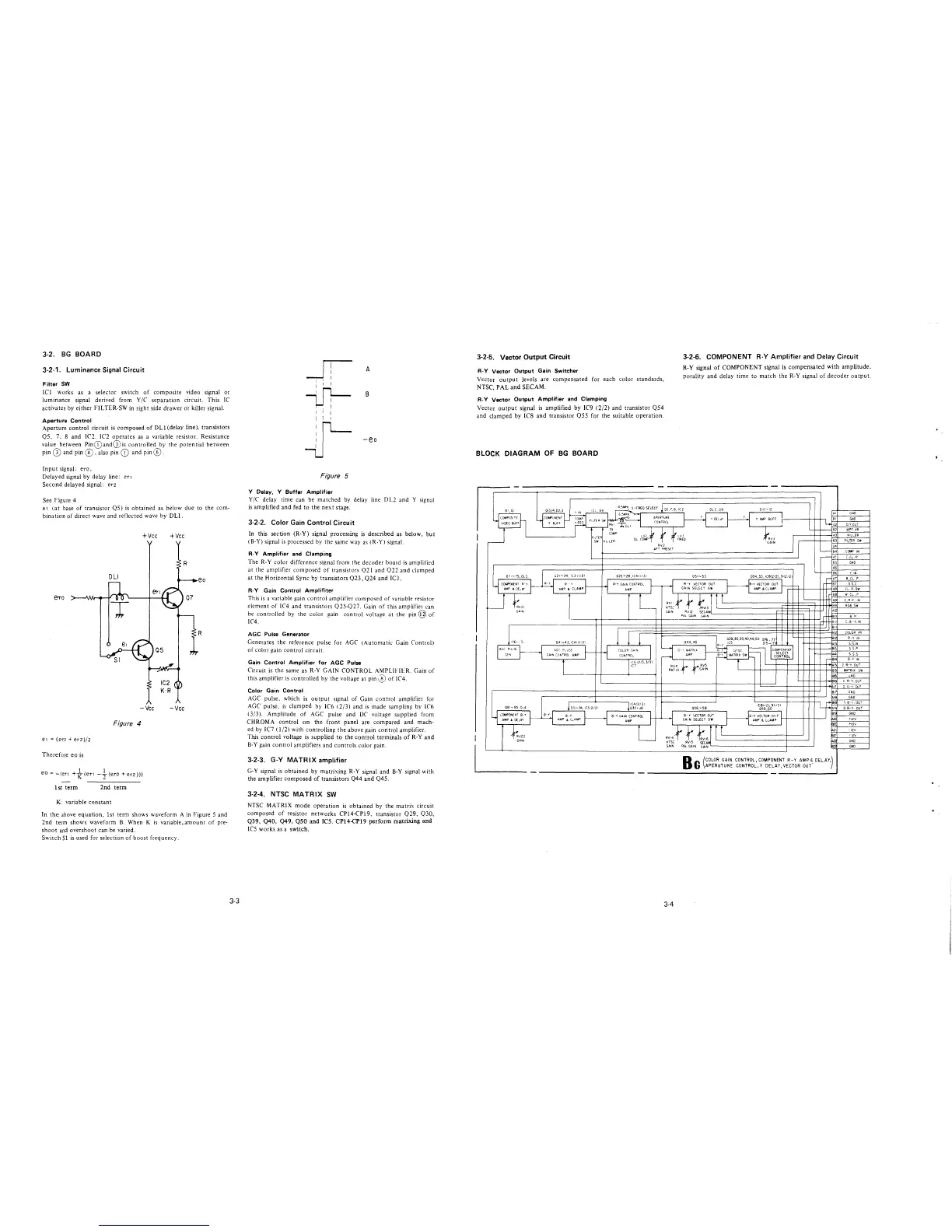
3-2. BG BOARD
3-2-1. Luminance Signal Circuit
Filter SW
!CI works as a selector switch of composite video signal or
luminance signal derived from Y /C separation circuit. This IC
activates by either FILTER-SW in right side drawer or killer signal.
Aperture Control
Aperture control circuit is composed of DLl (delay line), transistors
Q5, 7, 8 and IC2. IC2 operates as a variable resistor. Resistance
value between Pin(DandG)is controlled by the potential between
pin 0 and pin © , also pin (D and pin© .
Input signal: eTo,
Delayed signal by delay line: eT 1
Second delayed signal: e72
See Figure 4
e1 (at base of transistor Q5) is obtained as below due to the com-
bination of direct wave and reflected wave by DLI.
+Vee
+Vee
eo
e-ro
05
-Vee -Vee
Figure 4
e1 = (ero + e72)/2
Therefore eo is
eo = -(m +1[ (eT1 -{ (eTO + e72 )})
1st term
2nd term
K: variable constant
In the above equation, 1st term shows waveform A in Figure 5 and
2nd term shows waveform B. When K is variable,amount of pre·
shoot and overshoot can be varied.
Switch S1 is used for selection of boost frequency.
3-3
-Ii
I '
-{Ji-
' I
I I I
t-
Figure 5
Y Delay, Y Buffer Amplifier
A
B
-eo
Y/C delay time can be matched by delay line DL2 and Y signal
is amplified and fed to the next stage.
3-2-2. Color Gain Control Circuit
In this section (R-Y) signal processing is described as below, but
(8-Y) signal is processed by the same way as (R-Y) signal.
R-Y Amplifier and Clamping
The R-Y color difference signal from the decoder board is amplified
at the amplifier composed of transistors 021 and 022 and clamped
at the Horizontal Sync by transistors Q23, Q24 and IC3.
R-Y Gain Control Amplifiter
This is a variable gain control amplifier composed of variable resistor
element of IC4 and transistors 025-027. Gain of this amplifier can
be controlled by the color gain control voltage at the pin@ of
IC4.
AGC Pulse Generator
Generates the reference pulse for AGC (Automatic Gain Control)
of color gain control circuit.
Gain Control Amplifier for AGC Pulse
Circuit is the same as R-Y GAIN CONTROL AMPLll·IER. Gain of
this amplifier is controlled by the voltage at pin® of IC4.
Color Gain Control
AGC pulse, which is output signal of Gain control amplifier for
AGC pulse, is clamped by IC6 ( 2/3) and is made sampling by 1C6
(3/3). Amplitude of AGC pulse and DC voltage supplied from
CHROMA control on the front panel are compared and mach-
ed by IC7 ( 1/2) with controlling the above gain control amplifier.
This control voltage is supplied to the control terminals of R-Y and
8-Y gain control amplifiers and controls color gain.
3-2-3. G-Y MATRIX amplifier
G-Y signal is obtained by matrixing R-Y signal and 8-Y signal with
the amplifier composed of transistors Q44 and Q45.
3-2-4. NTSC MATRIX SW
NTSC MATRIX mode operation is obtained by the matrix circuit
composed of resistor networks CPI4-CP19, transistor 029, 030,
Q39, Q40, Q49, QSO and IC5. CP14-CP19 perform matrixing and
!CS works as a switch.
I
3-2-5. Vector Output Circuit
3-2-6. COMPONENT R-Y Amplifier and Delay Circuit
R-Y Vector Output Gain Switcher
Vector output levels are compensated for each color standards,
NTSC, PAL and SECAM.
R-Y signal of COMPONENT signal is compensated with amplitude,
porality and delay time to match the R-Y signal of decoder output.
R-Y Vector Output Amplifier and Clamping
Vector output signal is amplified by IC9 (2/2) and transistor Q54
and clamped by IC8 and transistor Q55 for the suitable operation.
BLOCK DIAGRAM OF BG BOARD
-
-
01 ,01
~
4
.5MHi S1 FREQ SELECT
05, 7,8, 1(2
DL 2, 09
6~
~
l
COMPOS1Tf
I
APERTURE
y
Y OEL.il.Y
v10fo eurr
r1LTER SW r;;;
Tc,, l
CONTROL
I -~ DL
COMP
cv, f
f f LV'
FILTER
DL COMP
~REO
SW
l<.iLLfR
'¥2
APT PRESET
4 """"·"'~'"""·'""'"
025-28,1(411/3)
051-5.3
COMPONENT R-Y R-Y R Y
~
1
R-Y GAIN CONTROL
r--~
R. y VECTOR our
AMP & OE~AY AMD a (LAMP
,.P
GAIN SELECT SW
~
t,,
~::,~t .t tJ
I
GA1N
PAL GAIN
GAIN
~
l
j
041-.43,1(4131.31 044,45
R·Y
AGC PLUS£
~
-H
COLOR GA1N
I
G-r MATRIX G·Y
'
SE
GAIN CONTROL AMP
(QNrnOL
A"P
8·\
r
•c612/3,3/3l
'"
RV4 t }RVS
RATIO GAIN
1(4(2/31
""""°"~
Q3J.,..34,IC3t2/2l
035~ 38
056 --58
1 COMPONENT 8·Y 8-Y
8·Y
8-Y GAIN CONTROL
~
-Y
8 • Y VECTOR OUT
AMP & DELAY
AMP & (._AMP
••P
GAIN SELECT SW
;(.vzz
L
:~,,~t t
i
Rv,~J
GAIN
SECA
-
010 ... 12
Al GND
y
Y AMP BUH
9,
GNO
I
L. 42 O.Y.OUT
f.vJ
-~
~
82
IAPT.VR
A3
l<ILLER
I
GAIN
83
FILTER SW
A4
-
84
COMP IN
-
"
C.CL.P
BS GNO
A6
--
86
Y,IN
054, 55, 1(8(2121, 9(2/2)
~
A7 B.CL P
R-Y VECTOR OUT r-r=: -
t- 87
ss.c
AMP .8. (LAMP
AB CL.P.SW
88 W CL. r
A9 C.R-Y. IN
89
RGB. SW
"
+
R~ 8. p
.,,
C.8-Y.IN
8,i
I COLOR VR
029,30,39, 40, 49,50
D76, 77
812
R-Y tN
,cs
D15-17 _..._
I
S.S.N
1HSC
COMPONENT
~-
-
813 ss.P
MATRIX SW
SELECT
--
·~
S.S S
CONTROL
t
-
-~·
B·Y IN
Al
C R·Y. OUT
81
MATRIX SW
Ai6
GNO
I
V R·Y. OUT
17 D G Y. QIJT
81 GNO
A,
GNO
1(811/2),9!1/2)
T
'"
'r. 8-\. OUT
059,60
"
D e~v OUT
8-Y VE(TOR OIJT
81 GNO
AMP Ii, C.LAMP
"'
tl2V
""
+-1cv
A21
-12v
"'
-12v
"'
GNO
L
r
GAIN
PAL GAIN
GAIN
~
GNO
Be
(COLOR GAIN CONTROL, COMPONENT R-Y AMP 8: DELAYY
APERUTURE CONTROL,Y DELAY,VECTOR OUT
-
-
-
3-4