– 9 –
SECTION 6
DIAGRAMS
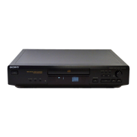
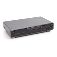
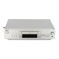
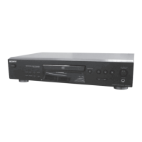
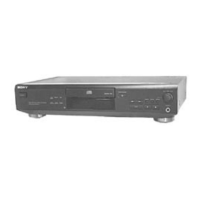
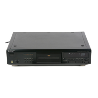
6-1. CIRCUIT BOARDS LOCATION
– 10 –
6. Check the level B of the oscilliscope's waveform and the A (DC
voltage) of the center of the Traverse waveform.
Confirm the following :
A/B x 100 = less than ± 7%
Traverse waveform
7. Press the “8” button. (The tracking servo is turned ON.) Confirm
the C (DC voltage) is almost equal to the A (DC voltage) is step
6.
Traverse waveform
8. Disconnect the lead wire of TP3 (ADJ) connected in step 1.
Adjustment Location :
[ BD BOARD ] — Side A —
[ MAIN BOARD ] — Component Side —
0V
C (DC
voltage)
Tracking servo
OFF
Tracking servo
ON
0V
level : 500
±
100 mVp-p
A (DC voltage)
Center of the waveform
B
MAIN board
PANEL board
LOADING board
POWER SW board
BD board
THIS NOTE IS COMMON FOR PRINTED WIRING
BOARDS AND SCHEMATIC DIAGRAMS.
(In addition to this, the necessary note is printed
in each block.)
For schematic diagrams.
Note:
• All capacitors are in µF unless otherwise noted. pF: µµF
50 WV or less are not indicated except for electrolytics
and tantalums.
• All resistors are in Ω and
1
/4
W or less unless otherwise
specified.
•
¢
: internal component.
• C : panel designation.
• U : B+ Line.
• V : B– Line.
• H : adjustment for repair.
• Voltages and waveforms are dc with respect to ground
under no-signal (detuned) conditions.
no mark : STOP
( ) : PLAY
∗
: can not to be measured
• Voltages are taken with a VOM (Input impedance 10 MΩ).
Voltage variations may be noted due to normal produc-
tion tolerances.
• Waveforms are taken with a oscilloscope.
Voltage variations may be noted due to normal produc-
tion tolerances.
• Circled numbers refer to waveforms.
• Signal path.
J : CD
c : digital out
Note: The components identified by mark ! or dotted line
with mark ! are critical for safety.
Replace only with part number specified.
For printed wiring boards.
Note:
• X : parts extracted from the component side.
• Y : parts extracted from the conductor side.
•
p : parts mounted on the conductor side.
•
®
: Through hole.
• b : Pattern from the side which enables seeing.
(The other layers' patterns are not indicated.)
IC103 @¶ MDP
1
2
3
4
5
WAVEFORMS
– CD SECTION –
IC101 #£ RFO
IC101 2 FEI
IC101 $¶ TEI
IC103 ^™ RFCK
6
IC103 ^º XPCK
7
IC103 &¢ WFCK
IC103 *ª XTAI
8
1
IC501 #¡ EXTAL
– PANEL SECTION –
500mV/DIV, 500nsec/DIV
1.3Vp-p
200mV/DIV, 1µsec/DIV
0.5Vp-p
50mV/DIV, 1msec/DIV
0.2Vp-p
7.8µsec
2.5Vp-p
135µsec
5Vp-p
135µsec
5Vp-p
16.9344MHz
2.6Vp-p
4MHz
4.2Vp-p
(VC)
(RF)
(FOK)
(TEO)
(FEO)
IC101
IC401
CN402
TP3 (JW41: ADJ)
TP2 (JW40: AF ADJ)
w
w
w
.
x
i
a
o
y
u
1
6
3
.
c
o
m
Q
Q
3
7
6
3
1
5
1
5
0
9
9
2
8
9
4
2
9
8
T
E
L
1
3
9
4
2
2
9
6
5
1
3
9
9
2
8
9
4
2
9
8
0
5
1
5
1
3
6
7
3
Q
Q
TEL 13942296513 QQ 376315150 892498299
TEL 13942296513 QQ 376315150 892498299
http://www.xiaoyu163.com
http://www.xiaoyu163.com