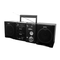
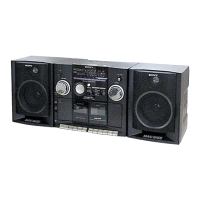
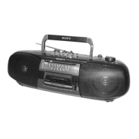
— 12 —
5-2. PRINTED WIRING BOARDS – TUNER SECTION –
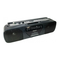
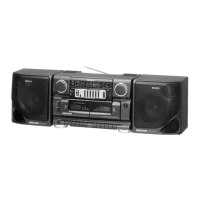
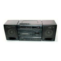
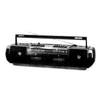
• Refer to page 11 for Circuit Boards Location.
THIS NOTE IS COMMON FOR PRINTED WIRING
BOARDS AND SCHEMATIC DIAGRAMS.
(In addition to this necessary note is printed in each
block)
For Schematic Diagrams.
Note:
• All capacitors are in µF unless otherwise noted. pF: µµF 50 WV or
less are not indicated except for electrolytics and tantalums.
• All resistors are in Ω and
1
/
4
W or less unless otherwise specified.
•
¢
: internal component.
• C : panel designation.
Note on Printed Wiring Boards:
• X : parts extracted from the component side.
• W : indicates side identified with part number.
• b : Pattern from the side which enables seeing.
• U : B+ Line.
• H : adjustment for repair.
• Power voltage is dc 9 V and fed with regulated dc power supply
from battery terminal.
• Voltages is dc with respect to ground under no-signal (detuned)
conditions.
no mark : FM
( ) : MW/SW
(( )) : PB
<< >>: REC
• Voltages are taken with a VOM (Input impedance 10 MΩ).
Voltage variations may be noted due to normal production toler-
ances.
• Signal path.
F : FM
E : PB
a : REC
L : SW1
g : SW2
f : MW
Note: The components identified by mark ! or dotted line
with mark ! are critical for safety.
Replace only with part number specified.
12
A
B
C
D
3456
Ref. No. Location
D1 B-5
D2 B-5
D3 B-2
IC1 C-3
Q1 B-2
Q2 D-4
• Semiconductor
Location
CFS-B7SMK2
w
w
w
.
x
i
a
o
y
u
1
6
3
.
c
o
m
Q
Q
3
7
6
3
1
5
1
5
0
9
9
2
8
9
4
2
9
8
T
E
L
1
3
9
4
2
2
9
6
5
1
3
9
9
2
8
9
4
2
9
8
0
5
1
5
1
3
6
7
3
Q
Q
TEL 13942296513 QQ 376315150 892498299
TEL 13942296513 QQ 376315150 892498299
http://www.xiaoyu163.com
http://www.xiaoyu163.com
 Loading...