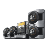
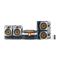
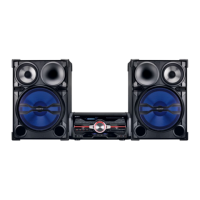
FST-GTK11iP/GTK33iP/RDH-GTK11iP/GTK33iP
FST-GTK11iP/GTK33iP/RDH-GTK11iP/GTK33iP
3737
For Schematic Diagrams.
Note:
• All capacitors are in μF unless otherwise noted. (p: pF) 50
WV or less are not indicated except for electrolytics and
tantalums.
• All resistors are in Ω and 1/4 W or less unless otherwise
specifi ed.
•
f
: Internal component.
• 2 : Nonfl ammable resistor.
• 5 : Fusible resistor.
• C : Panel designation.
THIS NOTE IS COMMON FOR PRINTED WIRING BOARDS AND SCHEMATIC DIAGRAMS.
(In addition to this, the necessary note is printed in each block.)
• A : B+ Line.
• Voltages and waveforms are dc with respect to ground
under no-signal (detuned) conditions.
no mark
: TUNER
( ) : iPod/iPhone
< > : DVD/PC IN
*
: Impossible to measure
• Voltages are taken with VOM (Input impedance 10 M).
Voltage variations may be noted due to normal production
tolerances.
• Waveforms are taken with a oscilloscope.
Voltage variations may be noted due to normal production
tolerances.
• Circled numbers refer to waveforms.
• Signal path.
F : TUNER
L : iPod/iPhone
G : USB
f : DVD/PC IN
For Printed Wiring Boards.
Note:
• X : Parts extracted from the component side.
• Y : Parts extracted from the conductor side.
•
f
: Internal component.
• : Pattern from the side which enables seeing.
(The other layers’ patterns are not indicated.)
Caution:
Pattern face side:
(Conductor Side)
Parts face side:
(Component Side)
Parts on the pattern face side seen
from the pattern face are indicated.
Parts on the parts face side seen from
the parts face are indicated.
• Indication of transistor.
C
B
These are omitted.
E
Q
• Abbreviation
SP6 : Singapore and Malaysia models
• Abbreviation
AUS : Australian model
E2 : 120V AC area in E model
E51 : Chilean and Peruvian models
EA : Saudi Arabia model
MX : Mexican model
RU : Russian model
SP6 : Singapore and Malaysia models
Caution:
Pattern face side:
(SIDE B)
Parts face side:
(SIDE A)
Parts on the pattern face side seen
from the pattern face are indicated.
Parts on the parts face side seen from
the parts face are indicated.
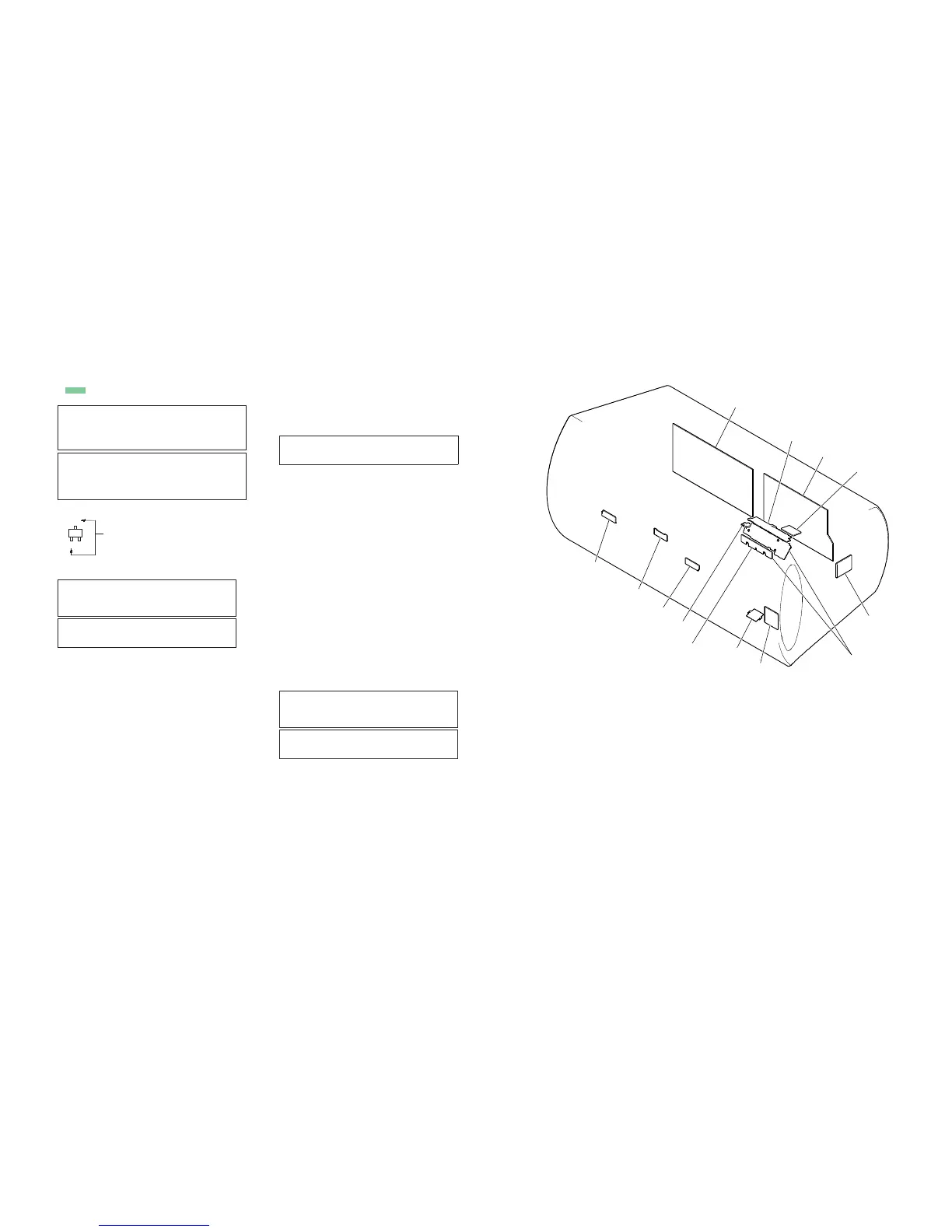
• Circuit Boards Location
Note: The components identifi ed by mark 0 or dotted
line with mark 0 are critical for safety.
Replace only with part number specifi ed.
Note 1: When the MAIN board is replaced, spread the com-
pound referring to “NOTE OF REPLACING THE
IC702 ON THE MAIN BOARD AND THE COM-
PLETE MAIN BOARD” on servicing notes (page 4).
Note 2: When the MAIN board is replaced, spread the bond
referring to “BOND FIXATION OF ELECTRIC
PARTS” on servicing notes (page 6).
GTK11-SMPS board (GTK11iP)/
GTK33-SMPS board (GTK33iP)
IP board
iPod board
RC board
LED board
tuner (TU1)
PANEL board
JUNCTION board
LED board
MAIN board
VOL JOG boar

 Loading...