D301 D-8
D302 G-5
D304 C-8
D314 I-5
D315 I-5
D317 B-8
D318 H-4
D319 B-7
D323 D-8
D324 E-4
D325 E-3
D361 F-4
D362 G-3
D651 D-1
D652 D-2
D801 F-1
D802 F-1
D810 C-5
D812 B-2
D813 C-1
D814 A-2
D815 F-1
D817 D-3
IC101 F-8
IC201 H-8
IC301 D-7
IC303 F-6
IC304 I-6
IC305 I-7
IC306 I-7
IC307 C-8
IC308 E-9
IC309 D-3
– 21 –
– 22 –
6-4. NOTE FOR PRINTED WIRING BOARDS AND SCHEMATIC DIAGARAMS
Note on Printed Wiring Board:
• X : parts extracted from the component side.
• Y : parts extracted from the conductor side.
• b : Pattern from the side which enables seeing.
Note on Schematic Diagram:
• All capacitors are in µF unless otherwise noted. pF: µµF
50 WV or less are not indicated except for electrolytics
and tantalums.
• All resistors are in Ω and
1
/
4
W or less unless otherwise
specified.
•
¢
: internal component.
• C : panel designation.
• U : B+ Line.
• V : B– Line.
• H : adjustment for repair.
• Voltages are taken with a VOM (Input impedance 10 MΩ).
Voltage variations may be noted due to normal produc-
tion tolerances.
• Waveforms are taken with a oscilloscope.
Voltage variations may be noted due to normal produc-
tion tolerances.
• Circled numbers refer to waveforms.
• Signal path.
F : TUNER
E : TAPE PLAY
a : TAPE RECORD
J : CD PLAY (ANALOG OUT)
c : CD PLAY (OPTICAL OUT)
• Abbreviation
CND : Canadian model
HK : Hong Kong model
MY : Malaysia model
SP : Singapore model
TH : Thai model
Note:
The components identi-
fied by mark ! or dotted
line with mark ! are criti-
cal for safety.
Replace only with part
number specified.
Note:
Les composants identifiés par
une marque ! sont critiques
pour la sécurité.
Ne les remplacer que par une
piéce portant le numéro
spécifié.
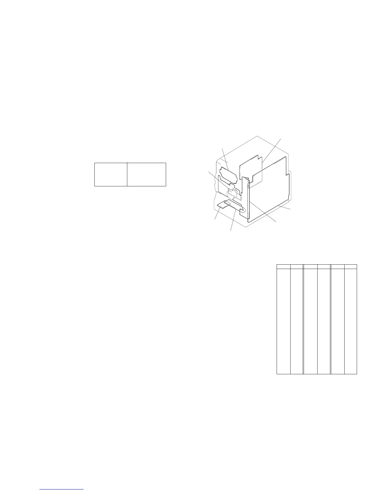
• Circuit Boards Location
LCD board
POWER board
MAIN boar
 Loading...