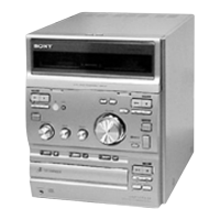
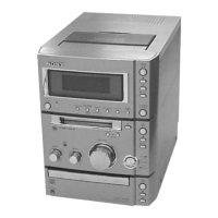
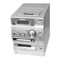
HCD-CP1
– 41 –
– 42 –
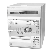
• Semiconductor
Location
Ref. No. Location
D902 C-3
D903 A-3
D904 A-4
D905 A-4
D906 A-4
D907 C-5
D908 C-5
D909 C-4
D910 C-5
D911 A-5
D912 B-5
D913 A-5
D914 A-5
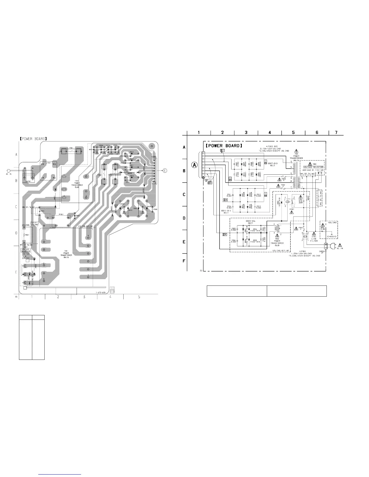
6-13. PRINTED WIRING BOARD – POWER Section –
• See page 22 for Circuit Boards Location.
6-14. SCHEMATIC DIAGRAM – POWER Section –
The components identified by mark ! or dotted
line with mark ! are critical for safety.
Replace only with part number specified.
Les composants identifiés par une marque ! sont
critiques pour la sécurité. Ne les remplacer que
par une piéce portant le numéro spécifié.
(Page 23)
(Page
28)