25
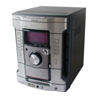
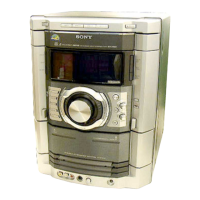
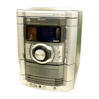
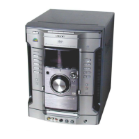
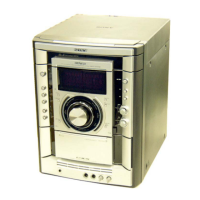
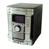
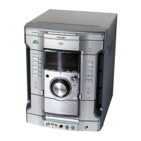
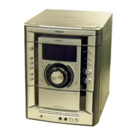
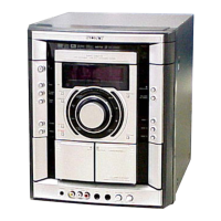
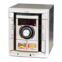
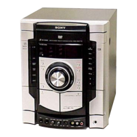
HCD-GN600
SECTION 7
DIAGRAMS
Note on Schematic Diagram:
• All capacitors are in µF unless otherwise noted. pF: µµF
50 WV or less are not indicated except for electrolytics
and tantalums.
• All resistors are in Ω and
1
/
4
W or less unless otherwise
specified.
• f : internal component.
•
2
: nonflammable resistor.
• 5 : fusible resistor.
Note on Printed Wiring Boards:
• X : parts extracted from the component side.
• : Pattern from the side which enables seeing.
(The other layers´ Patterns are not indicated.)
Caution:
Pattern face side: Parts on the pattern face side seen from the
(Side B) pattern face are indicated.
Parts face side: Parts on the parts face side seen from the
(Side A) parts face are indicated.
• Indication of transistor.
• C : panel designation.
• A : B+ Line.
• B : B– Line.
• H : adjustment for repair.
• Voltages and waveforms are dc with respect to ground
under no-signal conditions.
CD board section
no mark: CD PLAY
Other board section
no mark: TUNER (FM/AM)
( ): CD PLAY
< >: TAPE PLAY
[ ]: TAPE REC
• Voltages are taken with a VOM (Input impedance 10 MΩ).
Voltage variations may be noted due to normal produc-
tion tolerances.
• Waveforms are taken with a oscilloscope.
Voltage variations may be noted due to normal produc-
tion tolerances.
• Circled numbers refer to waveforms.
• Signal path.
F : TUNER (FM/AM)
E : TAPE PALY (DECK A)
d : TAPE PALY (DECK B)
G : RECORD
J : CD PALY (ANALOG OUT)
c : CD PALY (DIGITAL OUT)
q : MD/VIDEO (AUDIO) IN
j : GAME IN (AUDIO)
k : GAME IN (VIDEO)
N : MIC INPUT
Note:
The components identified by mark 0 or dotted line
with mark 0 are critical for safety.
Replace only with part number specified.
w
w
w
.
x
i
a
o
y
u
1
6
3
.
c
o
m
Q
Q
3
7
6
3
1
5
1
5
0
9
9
2
8
9
4
2
9
8
T
E
L
1
3
9
4
2
2
9
6
5
1
3
9
9
2
8
9
4
2
9
8
0
5
1
5
1
3
6
7
3
Q
Q
TEL 13942296513 QQ 376315150 892498299
TEL 13942296513 QQ 376315150 892498299
http://www.xiaoyu163.com
http://www.xiaoyu163.com