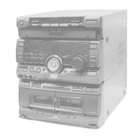
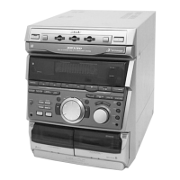
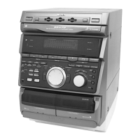
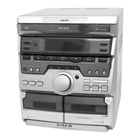
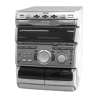
HCD-GR8000
SECTION 6
DIAGRAMS
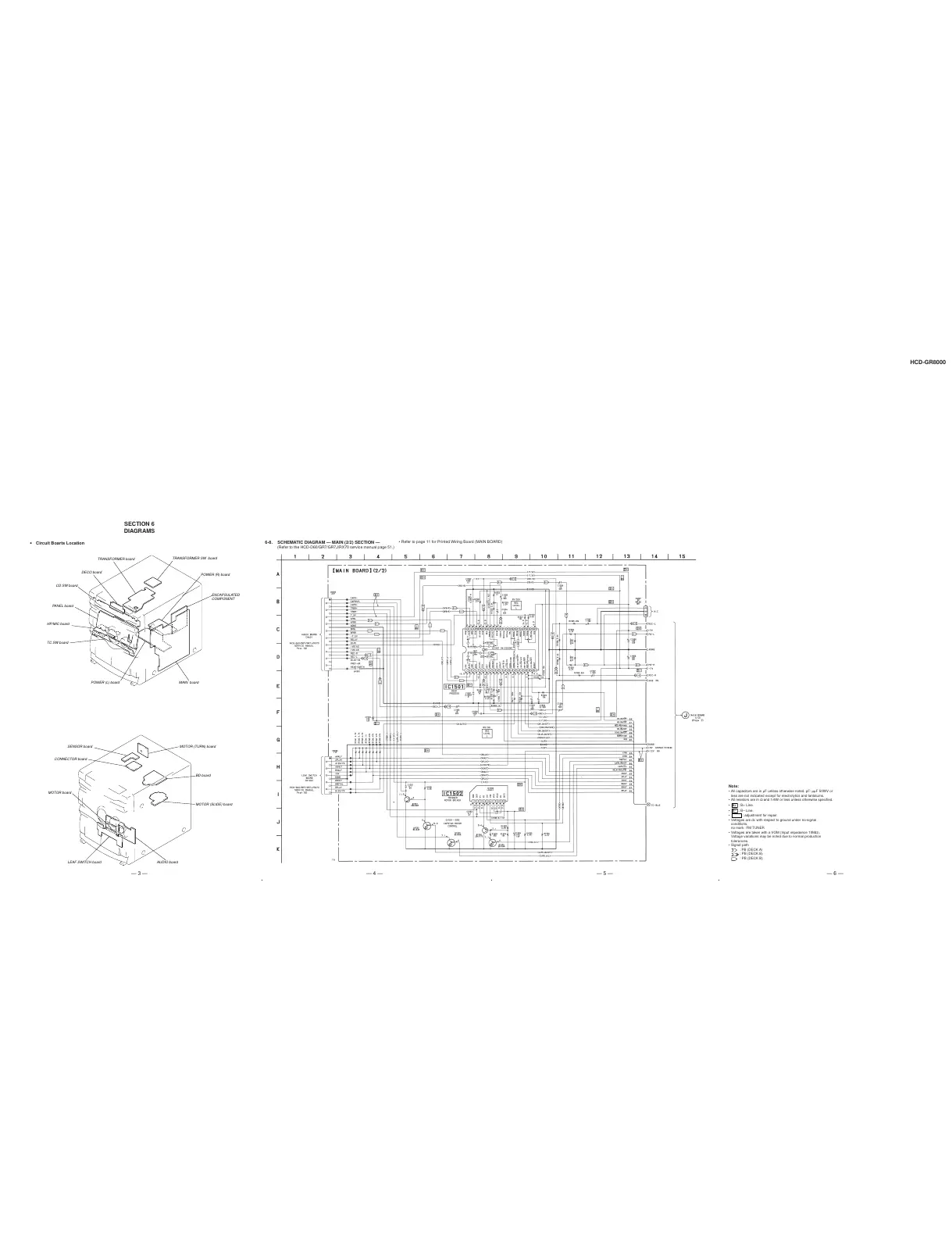
• Circuit Boarts Location
6-8. SCHEMATIC DIAGRAM — MAIN (2/2) SECTION —
(Refer to the HCD-D60/GR7/GR7J/RX70 service manual page 51.)
Note:
• All capacitors are in µF unless otherwise noted. pF: µµF 50WV or
less are not indicated except for electrolytics and tantalums.
• All resistors are in Ω and 1/4W or less unless otherwise specified.
•
B+
: B+ Line.
•
B–
: B– Line.
• : adjustment for repair.
•Voltages are dc with respect to ground under no-signal
conditions.
no mark : FM TUNER
•Voltages are taken with a VOM (Input impedance 10MΩ).
Voltage variations may be noted due to normal production
tolerances.
• Signal path
: PB (DECK A)
: PB (DECK B)
: PB (DECK B)
— 3 — — 4 — — 5 — — 6 —
• Refer to page 11 for Printed Wiring Board (MAIN BOARD)
PANEL board
HP/MIC board
TC SW board
CD SW board
DECO board
TRANSFORMER board
TRANSFORMER SW board
ENCAPSULATE