EasyManua.ls Logo

Sony HCD-GRX30 User Manual

Sony HCD-GRX30
68 pages
To Next Page IconTo Next Page
Page #1 background imageLoading...
Page #1 background image
HCD-GRX30/GRX30J/R550/RXD5
US Model
Canadian Model
HCD-RXD5
AEP Model
UK Model
HCD-R550/RXD5
E Model
HCD-GRX30/GRX30J
Australian Model
HCD-GRX30
Tourist Model
HCD-GRX30J
SERVICE MANUAL
MINI Hi-Fi COMPONENT SYSTEM
MICROFILM
Manufactured under license from Dolby Laboratories
Licensing Corporation.
“DOLBY” and the double-D symbol a are trademarks
of Dolby Laboratories Licensing Corporation.
HCD-GRX30/GRX30J/R550/RXD5 is
the Amplifier, CD player, Tape Deck and
Tuner section in MHC-GRX30/GRX30J/
R550/RXD5
— Continued on next page —
SPECIFICATIONS
Model Name Using Similar Mechanism HCD-GRX5/RX66
CD Mechanism Type CDM38LH-5BD32L
Base Unit Type BU-5BD32L
Optical Pick-up Type KSS-213D/Q-RP
Model Name Using Similar Mechanism HCD-GRX5
Tape Transport Mechanism Type TCM-230AWR2
CD
Section
TAPE
DECK
Section
AUDIO POWER SPECIFICATIONS:
POWER OUTPUT AND TOTAL
HARMONIC DISTORTION
US model:
with 6 ohm loads both channels driven, from 70 -
20,000 Hz; rates 60 watts per channel minimum RMS
power, with no more than 0.9% total harmonic
distortion from 250 milliwatts to rated output.
Amplifier section
North American model:
Continuous RMS power output (reference)
60 + 60 W
(6 at 1 kHz, 10% THD)
European model:
DIN power output (rated) 60 + 60 W
(6 at 1 kHz, DIN)
Continuous RMS power output (reference)
80 + 80 W
(6 at 1 kHz, 10% THD)
Music power output (reference)
140 + 140 W
(6 at 1kHz, 10% THD)
Other models:
The following measured at AC 110, 220 V 50/60 Hz
DIN power output (rated)60 + 60 W
(6 at 1 kHz, DIN)
Continuous RMS power output (reference)
80 + 80 W
(6 at 1 kHz, 10% THD)
The following measured at AC 120, 240 V 50/60 Hz
DIN power output (rated)70 + 70 W
(6 at 1 kHz, DIN)
Continuous RMS power output (reference)
100 + 100 W
(6 at 1 kHz, 10% THD)
Inputs
MD/VIDEO (AUDIO) IN:
(phono jacks) voltage 450 mV/250mV,
impedance 47 k
MIX MIC: (phone jack) sensitivity 1 mV,
impedance 10 k
Outputs
MD/VIDEO (AUTO) OUT:
(phono jack) voltage 250 mV
impedance 1 k
PHONES: accepts headphones of 8
(stereo mini jack) or more
SPEAKER: accepts impedance of 6 to
16
SUPER WOOFER
(except for European model):
Voltage 1V, impedance 1k
CD player section
System Compact disc and digital audio
system
Laser Semiconductor laser (λ=780nm)
Emission duration: continuous
Laser output Max. 44.6 µW*
*This output is the value
measured at distance of 200 mm
from the objective lens surface on
the Optical Pick-up Block with 7
mm aperture.
Frequency response 2 Hz - 20 kHz (±0.5 dB)
Wavelength 780 -790 nm
Signal-to-noise ratio More than 85 dB
Dynamic range More than 85 dB
CD OPTICAL DIGITAL OUT
(Square optical connector jack, rear panel)
Wavelength 600 nm
Output Level –18 dBm
Photo: HCD-GRX30
Question and Answer IconNeed help?

Do you have a question about the Sony HCD-GRX30 and is the answer not in the manual?

Sony HCD-GRX30 Specifications

General IconGeneral
TypeMini Hi-Fi Component System
CD PlayerYes
Cassette DeckYes
Speakers2-way speakers
Weight (main unit)4.5 kg
TunerAM/FM

Summary

Specifications

Audio Power Specifications

Details power output and total harmonic distortion.

CD Player Section Specifications

Lists specifications for the CD player system, laser, etc.

General Specifications

Power Requirements and Consumption

Specifies AC voltage, frequency, and power consumption for different models.

Tape Player Section Specifications

Recording System and Frequency Response

Describes the recording system and frequency response.

Tuner Section Specifications

FM Tuner Section Details

Details tuning range, antenna, and intermediate frequency.

AM Tuner Section Details

Provides tuning range and antenna details for AM bands.

Section 1 Servicing Notes

Handling Optical Pick-Up Block

Precautions for handling the optical pick-up block to prevent electrostatic breakdown.

Laser Diode Emission Check

Guidelines for safely checking laser diode emission to avoid eye damage.

Chip Component Replacement Notes

Advises against reusing chip components and cautions about tantalum capacitors.

Flexible Circuit Board Repairing

Provides instructions and cautions for repairing flexible circuit boards.

Section 3 Disassembly Procedures

3-1. Case Disassembly

Step-by-step instructions for disassembling the main case of the unit.

3-2. Front Panel Section Disassembly

Procedure for removing and disassembling the front panel section.

3-3. Tape Mechanism Deck Disassembly

Procedure for disassembling the tape mechanism deck.

3-4. CD Mechanism Deck Disassembly

Procedure for disassembling the CD mechanism deck.

3-5. Main Board Access

Steps for removing and accessing the main board.

Safety Check-Out Procedures

AC Leakage Check

Instructions for checking AC leakage from metal parts to ensure safety.

Model Identification

Back Panel Identification

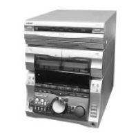
Information on identifying the model by checking the back panel and part numbers.

Section 2 General Information

Control Panel Overview

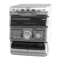
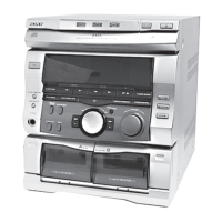
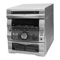
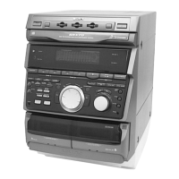
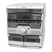
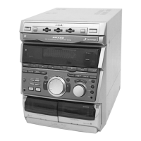
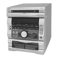
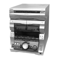
Identifies and describes the various buttons and indicators on the front panel.

Section 4 Test Modes

MC Cold Reset Procedure

Procedure to reset the unit to initial conditions, clearing all preset data.

CD Delivery Mode

Mode to position the pickup for vibration resistance during shipping.

MC Hot Reset Procedure

Resets the unit without clearing preset data, similar to power cycling.

Sled Servo Mode Operation

Allows free movement of the CD sled motor for cleaning or adjustments.

AM Tuner Step Change

How to change the AM channel step between 9 kHz and 10 kHz.

All Lit and Key Check Mode

Mode to test all LEDs and indicator tubes, and check key input functions.

Aging Mode Operation

Mode used for checking CD and tape deck operation over time.

Section 5 Mechanical Adjustments

Mechanical Adjustment Precautions

General precautions before performing mechanical adjustments.

Torque Measurement Specifications

Specifications for torque measurements on various tape deck components.

Section 6 Electrical Adjustments

Deck Section Adjustments

Settings and test tapes for deck section adjustments.

Record/Playback Head Azimuth Adjustment

Procedure for adjusting the azimuth of record/playback heads for both decks.

Tape Speed Adjustment (Deck B)

Steps for adjusting tape speed on Deck B using test tapes.

Playback Level Adjustment

Procedure for adjusting playback levels for both decks.

REC Bias Adjustment (Deck B)

Procedure for adjusting recording bias on Deck B.

REC Level Adjustment (Deck B)

Procedure for adjusting recording level on Deck B.

CD Section Adjustments

S-Curve Check Procedure

How to check the S-curve waveform for focus adjustment.

E-F Balance Check

Procedure for checking E-F balance during a 1-track jump.

RF Level Check

Steps to check the RF signal level and waveform clarity.

RF PLL Free-run Frequency Check

Method to measure the free-run frequency of the RF PLL.

Section 7 Diagrams

7-1. Circuit Boards Location

Illustrates the physical location of various circuit boards within the unit.

7-2. Block Diagrams - CD Section

Block diagram illustrating the CD section's signal flow and components.

7-2. Block Diagrams - Tape Deck Section

Block diagram showing the signal path and components of the tape deck section.

7-2. Block Diagrams - Main Section

Block diagram detailing the main section's circuitry and interconnections.

7-2. Block Diagrams - Display/Key Con Section

Block diagram for the display and key control circuitry.

7-3. Printed Wiring Board - CD Section

Printed wiring board layout for the CD section (Side A and Side B).

7-4. Schematic Diagram - CD Section

Schematic diagram for the CD section, detailing electronic components and connections.

7-5. Printed Wiring Board - CD Motor Section

Printed wiring board layouts for CD motor control boards.

7-6. Schematic Diagram - CD Motor Section

Schematic diagrams for the CD motor control circuits.

7-7. Printed Wiring Board - Tape Deck Section

Printed wiring board layout for the tape deck section.

7-8. Schematic Diagram - Tape Deck Section

Schematic diagram for the tape deck section, showing circuitry.

7-9. Printed Wiring Board - Leaf SW Section

Printed wiring board layout for the leaf switch section.

7-10. Schematic Diagram - Leaf SW Section

Schematic diagram for the leaf switch section.

7-11. Printed Wiring Board - Main Section

Printed wiring board layout for the main section.

7-12. Schematic Diagram - Main Section (1/4)

Schematic diagram for the main section, part 1 of 4.

7-13. Schematic Diagram - Main Section (2/4)

Schematic diagram for the main section, part 2 of 4.

7-14. Schematic Diagram - Main Section (3/4)

Schematic diagram for the main section, part 3 of 4.

7-15. Schematic Diagram - Main Section (4/4)

Schematic diagram for the main section, part 4 of 4.

7-16. Printed Wiring Board - Panel Section

Printed wiring board layout for the panel section.

7-17. Schematic Diagram - Panel Section

Schematic diagram for the panel section.

7-18. Printed Wiring Board - AC Sec Standby Section

Printed wiring board layout for the AC sec standby section.

7-19. Schematic Diagram - AC Sec Standby Section

Schematic diagram for the AC sec standby section.

7-20. Printed Wiring Board - CD SW Section

Printed wiring board layout for the CD SW section.

7-21. Schematic Diagram - CD SW Section

Schematic diagram for the CD SW section.

7-22. IC Block Diagrams - BD Board

IC block diagram for the BD board (CXD2587Q).

7-23. IC Pin Function Description - Main Board

Pin function description for IC501 on the main board.

IC Pin Function Description

Pin function description for ICs on the main board.

IC Pin Function Description (Panel Board)

Pin function description for IC601 on the panel board.

Section 8 Exploded Views

8-1. Case Section Exploded View

Exploded view and parts list for the case section.

8-2. Front Panel Section Exploded View

Exploded view and parts list for the front panel section.

8-3. Chassis Section Exploded View

Exploded view and parts list for the chassis section.

8-4. CD Mechanism Deck Section 1

Exploded view and parts list for CD mechanism deck section 1.

8-5. CD Mechanism Deck Section 2

Exploded view and parts list for CD mechanism deck section 2.

8-6. Base Unit Section Exploded View

Exploded view and parts list for the base unit section.

8-7. Tape Mechanism Deck Section 1

Exploded view and parts list for tape mechanism deck section 1.

8-8. Tape Mechanism Deck Section 2

Exploded view and parts list for tape mechanism deck section 2.

Section 9 Electrical Parts List

ST-BY Board Parts List

Related product manuals