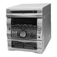
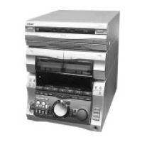
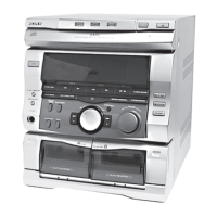
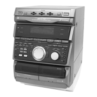
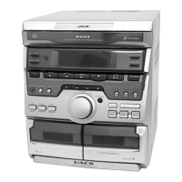
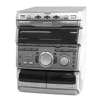
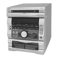
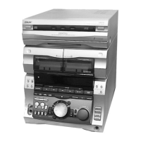
HCD-GRX50/R770/RXD7
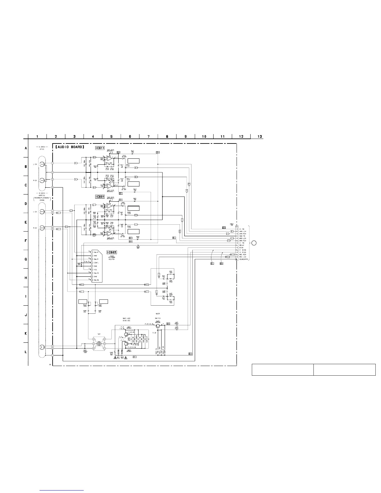
PB LEVEL (L)
(DECK A)
PB LEVEL (R)
(DECK A)
PB LEVEL (L)
(DECK B)
PB LEVEL (R)
(DECK B)
PB EQ AMP
(DECK A)
PB EQ AMP
(DECK B)
SWITCHING
REC BIAS (L)
(DECK B)
REC BIAS (R)
(DECK B)
BIAS OSC
REC BIAS
-6.8
(PLAYBACK)
D
– 39 –
– 40 –
7-11. SCHEMATIC DIAGRAM – AUDIO Board – • See page 66 for IC Block Diagram.
• Voltages are dc with respect to ground under no-signal
conditions.
no mark : TAPE PLAY
( ) : RECORD
The components identified by mark ! or dotted
line with mark ! are critical for safety.
Replace only with part number specified.
Les composants identifiés par une marque ! sont
critiques pour la sécurité. Ne les remplacer que
par une piéce portant le numéro spécifié.
(Page 49)
 Loading...