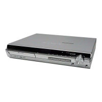
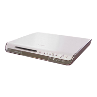
HCD-HDX285/HDX287WC/HDX585/HDX587WC/HDX589W/HDX685/HDX686W
79
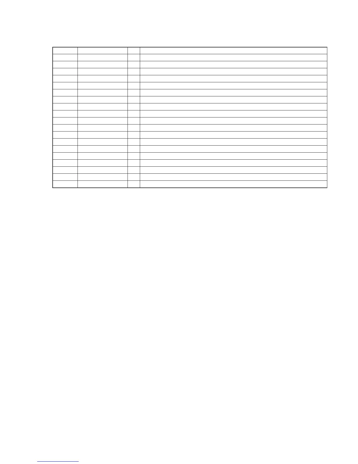
Pin No. Pin Name I/O Description
1 VSS - Ground terminal
2 NC - Not used
3 DATA I Serial data input from the system controller
4 CLK I Serial data transfer clock signal input from the system controller
5 LCK I Serial data latch pulse signal input from the system controller
6 Q0 O LED drive signal output terminal for DISC 5 indicator (green) "L": LED on
7 Q1 O LED drive signal output terminal for DISC 5 indicator (orange) "L": LED on
8 Q2 O LED drive signal output terminal for DISC 4 indicator (green) "L": LED on
9 Q3 O LED drive signal output terminal for DISC 4 indicator (orange) "L": LED on
10 Q4 O LED drive signal output terminal for DISC 3 indicator (green) "L": LED on
11 Q5 O LED drive signal output terminal for DISC 3 indicator (orange) "L": LED on
12 Q6 O LED drive signal output terminal for DISC 2 indicator (green) "L": LED on
13 Q7 O LED drive signal output terminal for DISC 2 indicator (orange) "L": LED on
14 Q8 O LED drive signal output terminal for DISC 1 indicator (green) "L": LED on
15 Q9 O LED drive signal output terminal for DISC 1 indicator (orange) "L": LED on
16, 17 Q10, Q11 - Not used
18 SO O Serial data output terminal Not used
19 X-OE I Output enable signal input terminal Not used
20 VDD - Power supply terminal (+3.3V)
KEY BOARD IC802 BU2099FV (LED DRIVER)
 Loading...