12
ICD-ST25
SECTION 4
DIAGRAMS
Note on Schematic Diagrams:
• All capacitors are in µF unless otherwise noted. pF: µµF
50 WV or less are not indicated except for electrolytics
and tantalums.
• All resistors are in Ω and
1
/
4
W or less unless otherwise
specified.
•
f
: internal component.
• C : panel designation.
• A : B+ Line.
•Power voltage is dc 3V and fed with regulated dc power
supply from DC IN jack (J5001).
•Voltages and waveforms are dc with respect to ground
under no-signal (detuned) conditions.
no mark : PB
[]: REC
∗
: Impossible to measure
•Voltages are taken with a VOM (Input impedance 10 MΩ).
Voltage variations may be noted due to normal produc-
tion tolerances.
•Waveforms are taken with a oscilloscope.
Voltage variations may be noted due to normal produc-
tion tolerances.
• Circled numbers refer to waveforms.
• Signal path.
F : PB
L : REC
✩Replacement of IC6001 used in this set requires a spe-
cial tool.
• The voltage and waveform of CSP (chip size package)
cannot be measured, because its lead layout is different
from that of conventional IC.
Caution:
Pattern face side: Parts on the pattern face side seen from
(SIDE B) the pattern face are indicated.
Parts face side: Parts on the parts face side seen from
(SIDE A) the parts face are indicated.
• MAIN board is multi-layer printed board. However, the
patterns of intermediate-layer have not been included in
the diagram.
✩Replacement of IC6001 used in this set requires a spe-
cial tool.
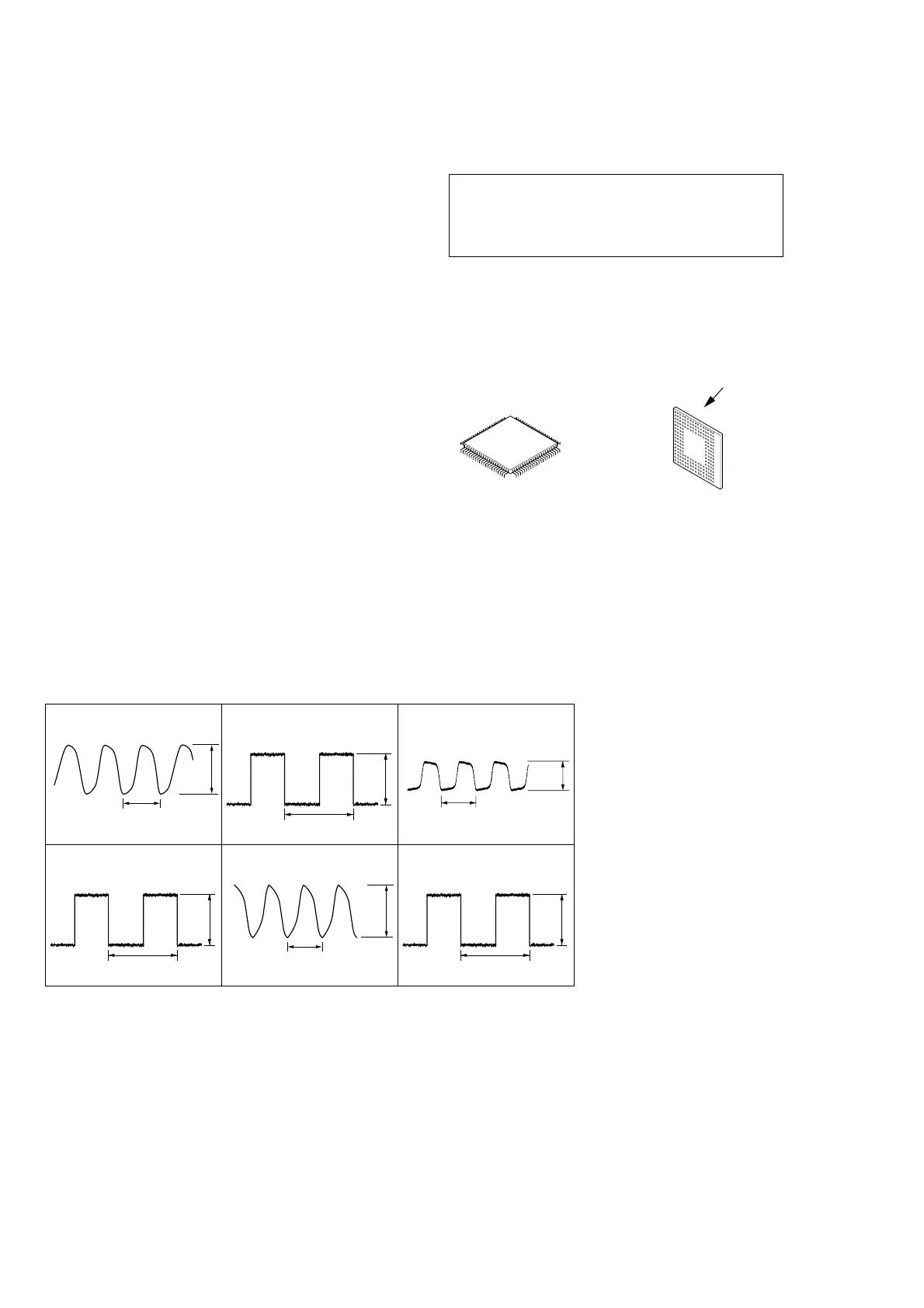
• Lead layouts
• WAVEFORMS
1 IC6003 3 (XXT)
2 IC6003 1 (FOUT)
3 IC3004 6 (MCLK)
4 IC7003 <z/, (XTAL)
5 IC8001 qd (X OUT)
(When the USB is connected)
6 IC7004 5 (FOUT)
1 V/DIV, 40 ns/DIV
3.3 Vp-p
88.5 ns
1 V/DIV, 40 ns/DIV
88.5 ns
4.1 Vp-p
1 V/DIV, 40 ns/DIV
88.5 ns
4.1 Vp-p
1 V/DIV, 100 ns/DIV
3.4 Vp-p
244 ns
1 V/DIV, 40 ns/DIV
3.7 Vp-p
8.33 ns
1 V/DIV, 10 µs/DIV
30.5 ns
3.2 Vp-p
Note on Printed Wiring Boards:
• Y : parts extracted from the conductor side.
• b : Pattern from the side which enables seeing.
The other layers’ patterns are not indicated.
surface
Lead layout of
conventional IC
CSP (chip size package)
 Loading...