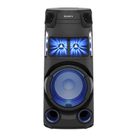
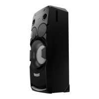
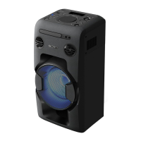
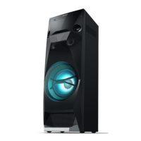
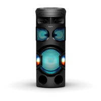
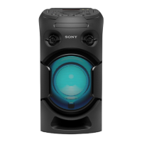
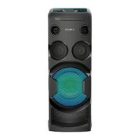
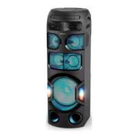
MHC-V3/V4D
68
• IC Pin Function Descriptions
ARAGON BOARD (6/6) IC101 R7S7200022CFP (SYSTEM CONTROLLER)
Pin No. Pin Name I/O Description
1 NC - Not used
2 VIDEO-MUTE O Muting Control for Video
3 CDM-UNLOAD-SW I CDM UNLOAD SW
4 CDM-LOAD-SW I CDM LOAD SW
5 BT-RESET O Reset signal output to the Bluetooth module “H”: reset
6 NC - Not used
7 Vcc - Power supply terminal (+3.3V)
8 BT-ON O Bluetooth on/off control signal output terminal for bluetooth section
9 Vss - Ground terminal
10 NC - Not used
11 PVcc -
Power supply terminal (+3.3V)
12 VBUS-OE O MTK Vbus Output enable control pin
13 NC - Not used
14 AUDIO_CLK_OUT O Clock Signal from Aragon to MTK master clock
15 MTK-RESET O MTK Reset pin
16 MTK-BUSY O BUSY Signal communication between MTK
17 MTK-CLK I Clock Signal from MTK
18 Vss - Ground terminal
19 MTK-XIFCS I MTK CHIP SELECT
20 MTK-SDI I Data In Signal from MTK
21 Vcc - Power supply terminal (+3.3V)
22 MTK-SDO O Data Out Signal to MTK
23 Vss - Ground terminal
24 SSI3_BCKO O Clock signal from Aragon to DAC BIT
25 PVcc - Power supply terminal (+3.3V)
26 SSI3_LRCKO O Clock signal from Aragon to DAC LRCK
27 NC - Not used
28 SSI3_DI I SRC from MTK to Aragon data in
29 SSI0_BCKO O Clock signal from Aragon to Wf DAC BCK
30 SSI0_LRCKO O Clock signal from Aragon to Wf DAC LRCK
31 Vss - Ground terminal
32 SSI0_DO O Data Out from Aragon to Wf DAC
33 SSI0_DI O Data out from Aragon to Tw DAC
34 Vcc - Power supply terminal (+3.3V)
35 LCD_CLK O Serial clock output to FL CIG
36 Vss - Ground terminal
37 CKIO - Not used
38 LCD_CSB O LCD Chip Select
39 PVcc - Power supply terminal (+3.3V)
40 LCD_SDA O Serial data output to LCD
41 ANALOG-ASEL O Multiplexer selector A for Analog input
42 ANALOG-BSEL O Multiplexer selector B for Analog input
43 DEBUG-TxD O TxD (for Debug)
44 NFC-SPICLK O Serial data transfer clock signal output to the NFC
45 POWER-KEY I Power Key input terminal
46 Vss - Ground terminal
47 USB-OC I USB Overcurrent Detection input port
48 BLUE_LED
O
Bluetooth LED control
49 NFC-SW O NFC standby control output terminal to the NFC section
50 PVcc - Power supply terminal (+3.3V)
51 NC - Not used
52 NFC-SEL O NFC data read/write control output terminal to the NFC section
53 NFC-RF-DET I NFC RF signal detection signal input from the NFC section
54 SSI1_DO O Data Out signal from Aragon to Tw DAC
Ver. 1.1