3
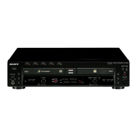
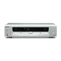
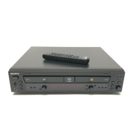
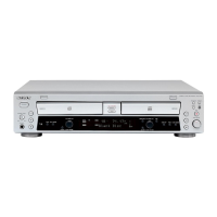
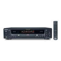
RCD-W500C
TABLE OF CONTENTS
1. SERVICING NOTE·····················································4
2. GENERAL ···································································5
3. DISASSEMBLY ··························································6
3-1. Case (409538) ······························································· 7
3-2. Loading Panel (CDR) ··················································· 7
3-3. Front Panel Section ······················································· 8
3-4. SW Board, LED Board, DISP Board···························· 8
3-5. CD Mechanism Deck (CDM65-RBD2) ······················· 9
3-6. Tray ··············································································· 9
3-7. CDR Board ································································· 10
3-8. Motor Assy (Loading) (M201) ··································· 10
3-9. Holder (MG) Sub Assy, Dust Cover ··························· 11
3-10. Optical Pick-Up (KRM-220CAA)······························ 11
3-11. Cam (CH)···································································· 12
3-12. MAIN Board ······························································· 12
3-13. CD Mechanism Deck (CDM53L-30B61M) ··············· 13
3-14. Fitting Base (Magnet) Assy ········································ 13
3-15. CLAMP MOTOR Board,
Motor (Clamp) Assy (M701) ······································ 14
3-16. Fitting Base (Guide) Assy, Bracket (Chassis) ············· 14
3-17. Tray (Sub) ··································································· 15
3-18. Chassis (Mold B) ························································ 15
3-19. LOAD MOTOR Board,
Motor (Loading) Assy (M702) ··································· 16
3-20. Stocker Section ··························································· 16
3-21. Slider (Selection), Tension Spring (Shutter),
Slider (Shutter)···························································· 17
3-22. Gear (Gear A), Gear (Gear B), Gear (U/D Slider) ······ 17
Precaution During Gear (Gear U/D Slider),
Gear (Gear B), Gear (Gear A) Installation·················· 18
3-23. Gear (Chucking) ························································· 18
3-24. BD Board ···································································· 19
3-25. Optical Block Section ················································· 19
4. TEST MODE ···································································· 20
5. ELECTRICAL ADJUSTMENTS
CD SECTION ····························································· 23
CD-R/RW SECTION·················································· 25
6. DIAGRAMS ······································································ 55
6-1. Block Diagrams – CD-R Section – ··························· 56
– CD Section – ······························· 57
– POWER/DISPLAY Section –······ 58
6-2. Printed Wiring Boards – BD Section – ······················· 59
6-3. Schematic Diagrams – BD Section –·························· 60
6-4. Printed Wiring Boards
– SENSER/MOTOR/SW Section – ····· 61
6-5. Schematic Diagrams
– SENSER/MOTOR/SW Section – ····· 62
6-6. Printed Wiring Boards – CD-R Section (Side A) – ···· 63
6-7. Printed Wiring Boards – CD-R Section (Side B) – ···· 64
6-8. Schematic Diagrams – CD-R Section (1/4) – ············· 65
6-9. Schematic Diagrams – CD-R Section (2/4) – ············· 66
6-10. Schematic Diagrams – CD-R Section (3/4) – ············· 67
6-11. Schematic Diagrams – CD-R Section (4/4) – ············· 68
6-12. Printed Wiring Boards – MAIN Section (Side A) – ··· 69
6-13. Printed Wiring Boards – MAIN Section (Side B) – ··· 70
6-14. Schematic Diagrams – MAIN Section (1/2) –············ 71
6-15. Schematic Diagrams – MAIN Section (2/2) –············ 72
6-16. Printed Wiring Boards – LED Section –····················· 73
6-17. Schematic Diagrams – LED Section – ······················· 74
6-18. Printed Wiring Boards – DISPLAY Section – ············ 75
6-19. Schematic Diagrams – DISPLAY Section – ··············· 76
6-20. IC Block Diagrams ····················································· 77
6-21. IC Pin Function Description ······································· 84
7. EXPLODED VIEWS
7-1. Case Section ·································································· 94
7-2. Front Panel Section ······················································· 95
7-3. Chassis Section ····························································· 96
7-4. Overall Section (CDM53L-30B61M) ··························· 97
7-5.
Chassis (Mold) Assy Section (CDM53L-30B61M)··········
98
7-6. Chassis Section (CDM53L-30B61M) ·························· 99
7-7. Base Unit Section (BU-30BBD61M) ························· 100
7-8. CDM65-RBD2 ···························································· 101
8. ELECTRICAL PARTS LIST ····································· 102
Unleaded solder
Boards requiring use of unleaded solder are printed with the lead-
free mark (LF) indicating the solder contains no lead.
(Caution: Some printed circuit boards may not come printed with
the lead free mark due to their particular size.)
: LEAD FREE MARK
Unleaded solder has the following characteristics.
• Unleaded solder melts at a temperature about 40°C higher than
ordinary solder.
Ordinary soldering irons can be used but the iron tip has to be
applied to the solder joint for a slightly longer time.
Soldering irons using a temperature regulator should be set to
about 350°C.
Caution: The printed pattern (copper foil) may peel away if the
heated tip is applied for too long, so be careful!
• Strong viscosity
Unleaded solder is more viscous (sticky, less prone to flow) than
ordinary solder so use caution not to let solder bridges occur such
as on IC pins, etc.
• Usable with ordinary solder
It is best to use only unleaded solder but unleaded solder may
also be added to ordinary solder.
 Loading...