SPP-A1070/A1071
1313
1
2 3
4
5 6 7 8
9
10
16 15 14 13 12
11
SHIFT REGISTER
LATCH
PARALLEL DATA
OUTPUT
GND
VCC
LATCH
CLOCK
PARALLEL DATA
OUTPUT
SERIAL DATA
INPUT
OUTPUT
ENABLE
SHIFT
CLOCK
SERIAL DATA
OUTPUT
RESET
QB
QC
QD
QE
QF
QG
QH
SQH
A
QA
+–
2
3
4
BIAS
CIRCUIT
+–
1
8
7
6
5
AMP1 AMP2
IN+
IN–
OUT1
VCC
GND
OUT2
MUTE
RIPPLE
REJECTION
1
3
4
5
6
9
10
12
24
23
22
21
20
19
18
17
16
15
14
13
SELECT
SWITCH
SERIAL
INTERFACE
+
–
+
–
CRYSTAL
OSCILLATOR
REFERENCE
GENERATOR
7
+
–
+
–
+
–
11
SELECT
ADC
BAND PASS FILTER CAS DETECTOR
FSK RECEIVERBAND PASS FILTER
BAND PASS FILTER
DIAL TONE
ENERGY DETECTOR
DIAL TONE
DETECTOR
RING DETECTOR
DC MEASUREMENT
UNIT
DC B
DC A
ADC
+
–
DTMF
GENERATOR
D/A CONVERSION
AND FILTERING
MDAT
SCK
SDIN
SDOUT
INT
RESET
VDDP
VDDA
DTMFOUT
OUTDC
INDCN
INDCP
DCB RD
VDDD
XIN
XOUT
VSSD
VREF
INSE
INP
OUT
VSSA
INN
8
2DCCOMPA
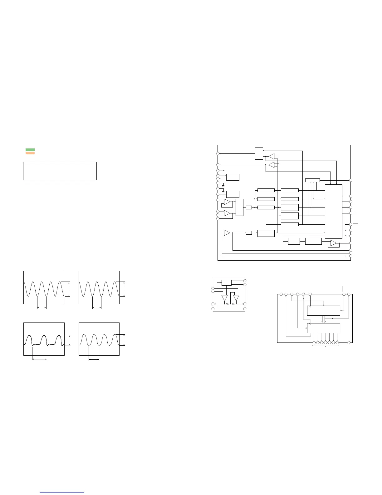
5-3. NOTE FOR PRINTED WIRING BOARDS AND SCHEMATIC DIAGRAMS
Note on Printed Wiring Board:
• X : parts extracted from the component side.
• Y : parts extracted from the conductor side.
•
z
: Through hole.
• : Pattern from the side which enables seeing.
• : Carbon pattern.
(The other layers' patterns are not indicated.)
Caution:
Pattern face side: Parts on the pattern face side seen from
(Conductor Side) the pattern face are indicated.
Parts face side: Parts on the parts face side seen from
(Component Side) the parts face are indicated.
Note on Schematic Diagram:
• All capacitors are in µF unless otherwise noted. pF: µµF
50 WV or less are not indicated except for electrolytics
and tantalums.
• All resistors are in Ω and
1
/
4
W or less unless otherwise
specified.
• % : indicates tolerance.
• C : panel designation.
• A : B+ Line.
• Power voltages are dc 9 V and fed with regulated dc power
supply from external power voltage jack (J3) on the BASE
MAIN board, dc 12 V and fed with regulated dc power
supply from modular jack (J1) on the BASE MAIN board
with 100 Ω in series, and dc 3.6 V and fed with regulated
dc power supply from battery terminal (J5) on the HAND
MAIN board.
• Voltages and waveforms are dc with respect to ground in
test mode.
∗
: Impossible to measure
• Voltages are taken with a VOM (Input impedance 10 MΩ).
Voltage variations may be noted due to normal produc-
tion tolerances.
• Waveforms are taken with a oscilloscope.
Voltage variations may be noted due to normal produc-
tion tolerances.
• Circled numbers refer to waveforms.
• Signal path.
N : RX
O : TX
P : BELL
2.4Vp-p
30.5 µs
3.9 Vp-p
125 ns
3.9 Vp-p
125 ns
• Waveforms
– BASE MAIN Board –
1 U4 qh (XOUT)
1 V/DIV, 50 ns/DIV
– HAND MAIN Board –
qa U2 3 (XOUT)
1 V/DIV, 50 ns/DIV
qs U2 7 (XTOUT)
1 V/DIV, 20 µs/DIV
1 Vp-p
279 ns
2 U3 5 (XOUT)
500 mV/DIV, 100 ns/DIV
• IC Block Diagrams
– BASE MAIN Board –
U3 PCC318
U9 KA8602D U10 SN74HC595ADBR