SPP-A1070/A1071
1717
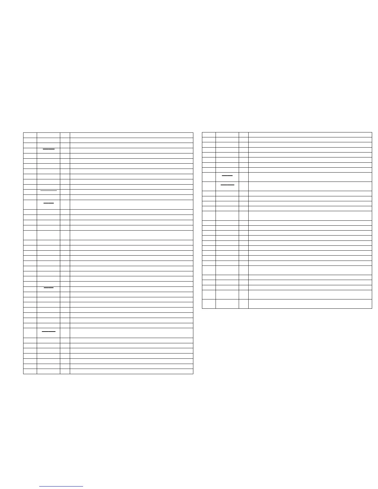
5-8. IC PIN FUNCTION DESCRIPTION
• BASE MAIN BOARD U4 TMP86CM25F-3CR3 (SYSTEM CONTROLLER)
Pin No. Pin Name I/O
Description
1 CIDSCL O Caller-ID clock signal output to the PCC318 (U3)
2 CIDSDA I/O Caller-ID two-way data bus with the PCC318 (U3)
3 CIDINT I Caller-ID interruption signal input from the PCC318 (U3) “L” active
4 DCB RD I Line DC input or ringer detection signal input from the PCC318 (U3)
5, 6 NC — Not used (open)
7 MESSAGE-LED O LED drive signal output of the MESSAGES indicator “L”: LED on Not used (open)
8
NEW CALL-LED
O LED drive signal output of the NEW CALL indicator (LED7) “L”: LED on
9 CHARGE-LED O LED drive signal output of the CHARGE indicator (LED5) “L”: LED on
10 IN USE-LED O LED drive signal output of the LINE indicator (LED6) “L”: LED on
11 NC — Not used (open)
12 OFF HOOK I Hook on/off control signal input terminal “L”: hook off, “H”: hook on
13 TEST I Setting terminal for the test Not used (fixed at “L”)
14 RESET I
System reset signal input terminal “L”: reset
For several hundreds msec. after the power supply rises, “L”: is input, then it changes to “H”
15 XIN I Main system clock input terminal (8 MHz)
16 XOUT O Main system clock output terminal (8 MHz)
17 VSS — Ground terminal
18 NC — Not used (fixed at “L”)
19 PLL EN O
Chip enable signal output to the RF unit
When PLL EN goes from “L” to “H”, it load data from PLL DATA
20 PLL CLK O Serial data transfer clock signal output to the RF unit
21 PLL DATA O Serial data output to the RF unit
22 NC — Not used (open)
23 CAR DET I Carrier detection signal input from the RF unit “L”: signal, “H”: no signal
24 TX DATA O Transmit data output to the RF unit
25 DI I Serial data input from the EEPROM (U6)
26 DO O Serial data output to the EEPROM (U6)
27 CLK O Serial data transfer clock signal output to the EEPROM (U6)
28 CS O Chip select signal output to the EEPROM (U6)
29 PARK I Charge detection signal input terminal “L”: charge on
30 FST CHG O Battery charge control signal output terminal
31 RX DATA I Receive data input from the RF unit
32 DVO O Not used (open)
33 PAGE I HANDSET LOCATOR switch (KP17) input terminal “H” input when key pressing
34 DCA I Line DC input from the PCC318 (U3)
35 NC — Not used (open)
36 ATE I/O I/O Communication in/out terminal with ATE program Not used (fixed at “L”)
37 CRADLE I
Detection signal input of the handset on cradle or off cradle “L”: on cradle, “H”: off cradle
Not used (open)
38 XTIN I Sub system clock input terminal (32.768 kHz) Not used (open)
39 XTOUT O Sub system clock output terminal (32.768 kHz) Not used (open)
40 VDD — Power supply terminal (+5V)
41 HSO O Not used (fixed at “L”)
42 HSCK O Not used (open)
43 SO O Not used (open)
44 SI I Caller-ID data input from the PCC318 (U3)
• HAND MAIN BOARD U2 TMP87C807U-3CR4 (SYSTEM CONTROLLER)
Pin No. Pin Name I/O
Description
1 VSS — Ground terminal
2 XIN I Main system clock input terminal (8 MHz)
3 XOUT O Main system clock output terminal (8 MHz)
4 TEST I Setting terminal for the test Not used (fixed at “L”)
5VDD— Power supply terminal (+3.6V)
6 XTIN I Sub system clock input terminal (32.768 kHz)
7 XTOUT O Sub system clock output terminal (32.768 kHz)
8 RESET I
System reset signal input terminal “L”: reset
For several hundreds msec. after the power supply rises, “L”: is input, then it changes to “H”
9 CRADLE I
Detection signal input of the handset unit on cradle or off cradle
“L”: on cradle, “H”: off cradle
10 ATE IO I/O Communication in/out terminal with ATE program Not used (pull down)
11 RX DATA I Receive data input from the RF unit
12 CAR DET I Carrier detection signal input from the RF unit “L”: signal, “H”: no signal
13 KEY INT O Key interruption signal output terminal
14 PLL EN O
Chip enable signal output to the RF unit
When PLL EN goes from “L” to “H”, it load data from PLL DATA
15 PLL CLK O Serial data transfer clock signal output to the RF unit
16 PLL I2C DATA I/O Two-way data bus with the RF unit and EEPROM (U4)
17 I2C CLK O Serial data transfer clock signal output to the EEPROM (U4)
18 VAREF I Reference voltage input terminal Not used (fixed at “L”)
19 to 21 COL0 to COL2 O Key scan output to the key matrix “L” output when key waiting
22 to 26 ROW0 to ROW4 I Key scan input from the key matrix “L” input when key pressing
27 BUZZER O Buzzer (BUZ1) drive signal output terminal
28 COL3 O Key scan output to the key matrix “L” output when key waiting
29 TX DATA O Transmit data output to the RF unit
30 BACKLIGHT O
LED drive signal output of the liquid crystal display module back light (D5, D6)
“L”: LED on
31 NC O Not used (pull up)
32 to 78 SEG0 to SEG46 O Segment drive signal output to the liquid crystal display module (LCD1)
79 to 94
COM0 to COM14
O Common drive signal output to the liquid crystal display module (LCD1)
95 to 98 V1 to V4 I
Input terminal for doubler circuit capacitor connection to develop liquid crystal display module
drive voltage
99, 100 C1, C2 I
Input terminal for doubler circuit capacitor connection to develop liquid crystal display module
drive voltage