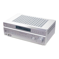
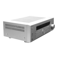
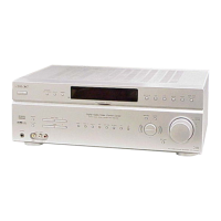
STR-KM22/KM55/KM77
59
MAIN BOARD (7/9) IC2106 MB9AF156NPMC-G-JNE2 (SYSTEM CONTROL)
Pin No. Pin Name I/O Description
1 VCC - Power supply pin (+3.3V)
2 DIR_INT I Interrupt status signal input from DIR
3 DIR_RST O Reset signal output to the digital audio interface receiver
4
DIR_CE
O Latch signal output for DIR IC
5 TUN_RDS_SIGNAL I RDS data signal input (for destination that support RDS only)
6 TUNER_MOSI O Serial data output to the tuner (FM/AM)
7 TUNER_CLK O Serial clock signal output for tuner pack
8
TUNER_CE
O Serial data latch pulse signal output to the tuner (FM/AM)
9 DAC_SDA I/O IIC data input/output from the D/A converter
10 DAC_SCL O IIC clock signal output to the D/A converter
11 BRIDGEABLE_RY O Relay drive signal (for power supply) output terminal “H”: relay on
12 SBL_SBR_RY O Relay drive signal (for surround back) output terminal “H”: relay on
13 SW_RY O Relay drive signal (subwoofer) output terminal “H”: relay on
14 FRONT_SPK_RY O Relay drive signal (for front) output terminal “H”: relay on
15 C/SL_SR_RY O Relay drive signal (for center and surround) output terminal “H”: relay on
16 EVOL_DATA O Serial data output to electrical volume
17 EVOL_CLK O Serial data transfer clock signal output to the electrical volume
18 PROTECT I Protect detection signal input terminal
19 E2P_SDA I/O Two-way data bus with the EEPROM
20 E2P_SCL O Serial data transfer clock signal output to the EEPROM
21 NO_USE - Not used
22 NO_USE - Not used
23
NO_USE
- Not used
24 LOT26_PCONT O Control Video mcu power
25 VSS - Ground terminal
26 VCC - Power supply pin (+3.3V)
27 BT_MUTE I Bluetooth: Mute request from BT device to Video uCOM
28
NO_USE
- Not used
29
NO_USE
- Not used
30 INPUT_LED O Input Jog LED Control
31 VOL_LED O Volume Jog LED Control
32 LED_BAR O LED BAR Control
33 C - Regulator stabilization capacity connecting pin
34
VSS
- Ground terminal
35 VCC - Power supply pin (+3.3V)
36
UART_SEL
O UART Selector
37
FAN_CTRL
O Fan ON/OFF Control
38 INITX I Main Micom Reset port
39 STOP I AC off detection signal input
40 POWER_RY O Power relay control signal output
41
FUSE_DET
I Fuse open detect signal input
42 FAN_BLK I Fan Fail Detect
43 FL_CLK O Clock signal output for FL DISPLAY DRIVER IC
44 FL_DATA O Serial data output for FL DISPLAY DRIVER IC
45
FL_LAT
O Latch signal output for FL DISPLAY DRIVER IC
46 MD1 - Selection of micon operation mode (Connect to VSS)
47 MD0 - Selection of micon operation mode (Connect to VSS)
48 X0 - Main oscillator connecting pin
49 X1 - Main oscillator connecting pin
50 VSS - Ground terminal
51 VCC - Power supply pin (+3.3V)
52 INPUT_JOG I Function encoder signal input
53 SIRCS_IN I SIRCS signal input
54 VOLUME_JOG I MASTER VOLUME encoder signal input
55 AD_KEY2 I Key signal input (A/D port)
 Loading...