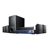
STR-KS2000
51
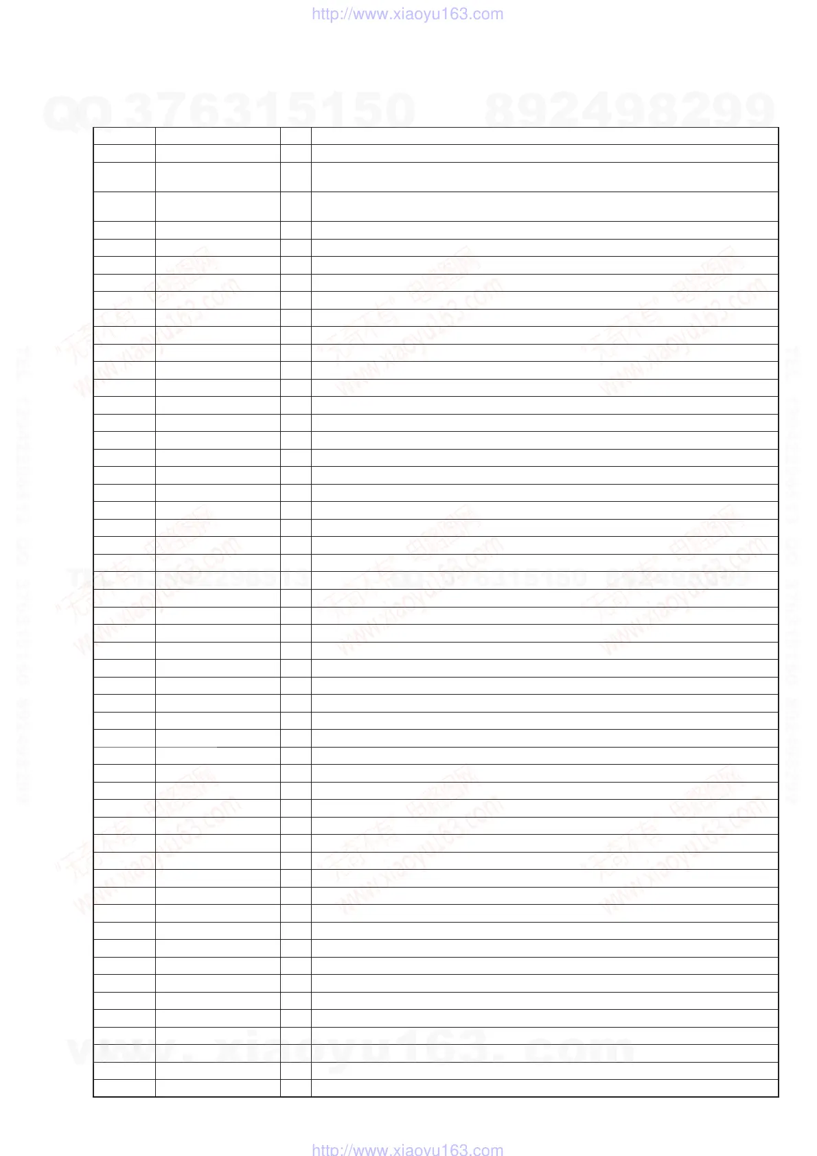
• IC Pin Function Description
MAIN BOARD IC1009 ADSST-AVR-1115 (DSP)
Pin No. Pin Name I/O Description
1 VDDINT - Power supply terminal (+1.2V)
2, 3
CLKCFG0,
CLKCFG1
I Clock frequency setting terminal
4, 5
BOOTCFG0,
BOOTCFG1
I Boot mode setting terminal for DSP
6 GND - Ground terminal
7 VDDEXT - Power supply terminal (+3.3V)
8 GND - Ground terminal
9 VDDINT - Power supply terminal (+1.2V)
10 GND - Ground terminal
11 VDDINT - Power supply terminal (+1.2V)
12 GND - Ground terminal
13 VDDINT - Power supply terminal (+1.2V)
14 GND - Ground terminal
15 DSP INT O Interrupt status output to the system controller
16 ERROR I PLL lock error signal and data error fl ag input terminal
17 AD7 I/O Two-way data bus and address signal output with S-RAM Not used
18 GND - Ground terminal
19 VDDINT - Power supply terminal (+1.2V)
20 GND - Ground terminal
21 VDDEXT - Power supply terminal (+3.3V)
22 GND - Ground terminal
23 VDDINT - Power supply terminal (+1.2V)
24 to 26 AD6 to AD4 I/O Two-way data bus and address signal output with S-RAM Not used
27 VDDINT - Power supply terminal (+1.2V)
28 GND - Ground terminal
29, 30 AD3, AD2 I/O Two-way data bus and address signal output with S-RAM Not used
31 VDDEXT - Power supply terminal (+3.3V)
32 GND - Ground terminal
33, 34 AD1, AD0 I/O Two-way data bus and address signal output with S-RAM Not used
35 XWR O Data write enable signal output to the S-RAM "L": active Not used
36, 37 VDDINT - Power supply terminal (+1.2V)
38 GND - Ground terminal
39 XRD O Read strobe signal output to the S-RAM "L": active Not used
40 ALE O Address latch enable signal output terminal Not used
41 to 43 AD15 to AD13 I/O Two-way data bus and address signal output with S-RAM Not used
44 GND - Ground terminal
45 VDDEXT - Power supply terminal (+3.3V)
46 AD12 I/O Two-way data bus and address signal output with S-RAM Not used
47 VDDINT - Power supply terminal (+1.2V)
48 GND - Ground terminal
49 to 52 AD11 to AD8 I/O Two-way data bus and address signal output with S-RAM Not used
53 A16 O Address signal output to S-RAM Not used
54 VDDINT - Power supply terminal (+1.2V)
55 GND - Ground terminal
56, 57 A17, A18 O Address signal output to S-RAM Not used
58 GND - Ground terminal
59 VDDEXT - Power supply terminal (+3.3V)
60 VDDINT - Power supply terminal (+1.2V)
61 GND - Ground terminal
62 PF_CE I/O Chip enable signal input/output terminal Not used
63 SPI_MAS O Master/slave selection signal output terminal "L": DSP is master
64 DPSOA O PCM audio signal (front L/R) output terminal
65 DPSOB O PCM audio signal (surround L/R) output terminal
66 VDDINT - Power supply terminal (+1.2V)
w
w
w
.
x
i
a
o
y
u
1
6
3
.
c
o
m
Q
Q
3
7
6
3
1
5
1
5
0
9
9
2
8
9
4
2
9
8
T
E
L
1
3
9
4
2
2
9
6
5
1
3
9
9
2
8
9
4
2
9
8
0
5
1
5
1
3
6
7
3
Q
Q
TEL 13942296513 QQ 376315150 892498299
TEL 13942296513 QQ 376315150 892498299
http://www.xiaoyu163.com
http://www.xiaoyu163.com