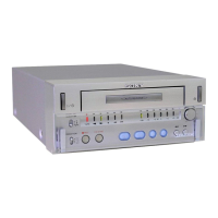
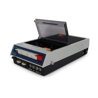
TC-SD1
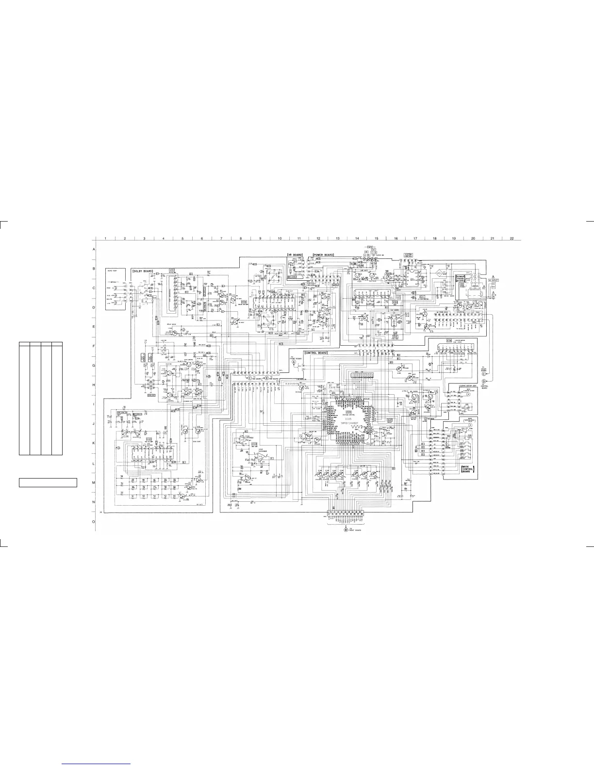
3-5. SCHEMATIC DIAGRAM — MAIN SECTION —
Note on Schematic Diagram:
• All capacitors are in µF unless otherwise noted. pF: µµF
50 WV or less are not indicated except for electrolytics
and tantalums.
• All resistors are in Ω and
1
/
4
W or less unless otherwise
specified.
• C : panel designation.
• U : B+ Line.
• V : B– Line.
• H : adjustment for repair.
• Voltages and waveforms are dc with respect to ground
under no-signal (detuned) conditions.
no mark : REC/PB
( ) : REC
< > : PB
[ ] : STOP
• Voltages are taken with a VOM (Input impedance 10 MΩ).
Voltage variations may be noted due to normal production
tolerances.
• Waveforms are taken with a oscilloscope.
Voltage variations may be noted due to normal production
tolerances.
• Circled numbers refer to waveforms.
• Signal path.
E : PB
a : REC
• Refer to page 25 for IC Block Diagrams. • Refer to page 27 for IC Pin Function Description. • Refer to page 15 for MODE CONTROL board Printed Wiring Board.
— 21 — — 22 — — 23 — — 24 —
Ref. No. Location
D01 F-5
D02 B-1
D03 B-7
D04 B-7
D05 E-9
D06 E-10
D07 D-12
D12 F-14
D13 C-1
D14 A-1
D15 C-3
D16 B-3
D17 E-12
D19 B-3
D20 C-3
D22 E-14
D23 E-14
D24 E-12
D25 E-12
D28 D-2
D36 F-14
D37 F-15
IC01 F-5
IC02 F-9
IC03 F-1
IC04 G-13
IC05 C-6
IC06 C-1
IC07 D-5
IC08 C-2
IC10 G-14
IC11 E-15
Q01 F-7
Q02 G-7
Q03 E-9
Q04 E-8
Q05 G-10
Q05A H-15
Q06 G-9
• Semiconductor Location
Ref. No. Location
Q06A G-14
Q07 G-5
Q08 G-4
Q09 F-3
Q10 G-4
Q11 G-4
Q12 G-3
Q12A G-3
Q13 F-3
Q13A G-3
Q14 E-1
Q15 F-1
Q16 G-2
Q17 G-2
Q18 G-2
Q19 B-2
Q20 D-11
Q21 B-3
Q22 C-2
Q23 C-2
Q24 C-2
Q25 D-2
Q26 C-3
Q27 D-3
Q29 C-7
Q30 C-7
Q31 C-7
Q32 C-7
Q33 C-7
Q34 D-7
Q35 C-6
Q36 C-6
Q37 B-12
Q38 C-7
Q39 G-12
Q40 G-12
Q41 H-13
Q42 B-12
Q43 C-13
Q44 E-14
Q45 G-10
Note: The components identified by mark ! or dotted line
with mark ! are critical for safety.
Replace only with part number specified.