3-1_
A BOARD
3-1-1. Composition
The A board consists
of
three
channels
of
video signal
amplifiers
that
include a
contrast
control
circuit,
pedestal clamp circuit,
output
amplifier (main),
and
blanking circuit. In
addition,
a sync signal
separator
and
various
control
pulse generators are also
located
on
the
A board. Each
of
the three AA boards,
mounted
on
the
A board, consists
of
a
contrast
ampli-
fier and clamp circuit. The
AB
board, also
mounted
on
the
A board, includes a sync signal
separator
and
c'ontrol pulse generators.
3-'
-2. Contrast Amplifier (AA Board)
The
contrast
control
amplifier utilizes a differential
amplifier for
current
balance
control
and a feedback
circuit
to
obtain
wide frequency response and
good
tracking
between
channels.
In
this circuit,
the
ampli-
fier gain can be
continuously
changed by
DC
adjust-
ment
for
contrast
control.
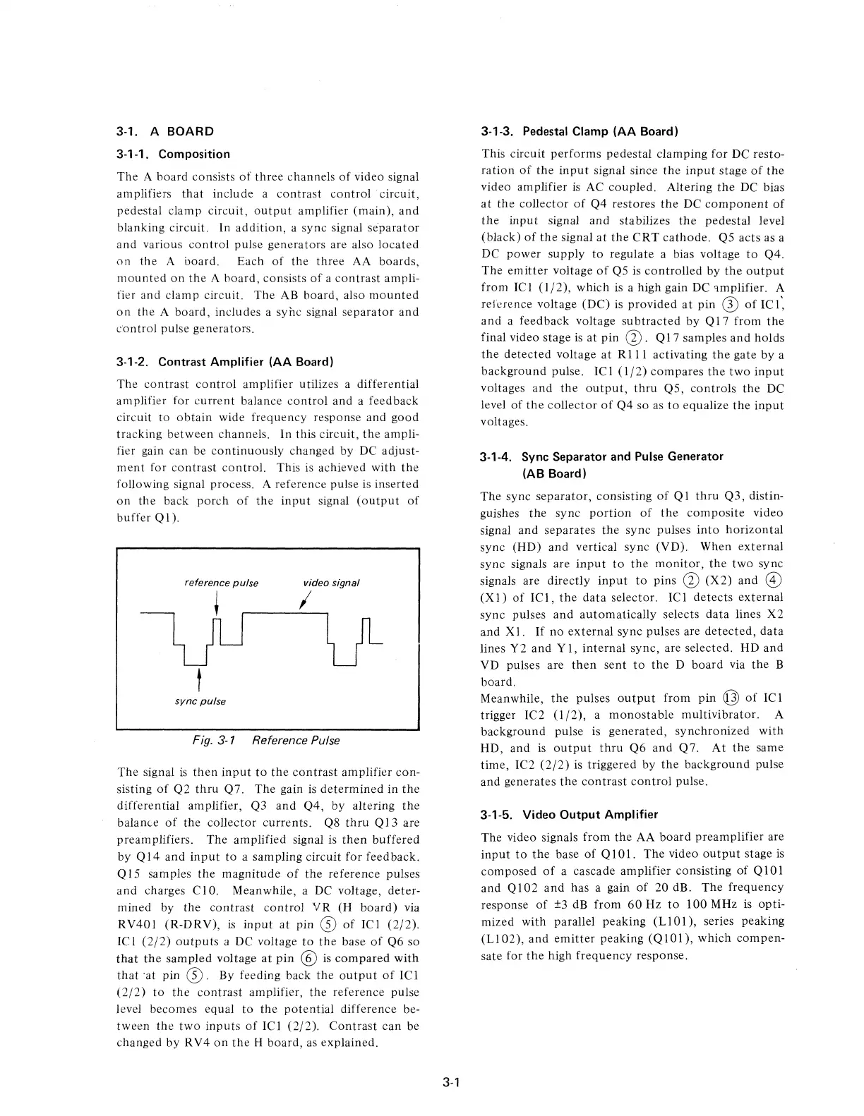
This is achieved with
the
following signal process. A reference pulse is inserted
on
the
back
porch
of
the
input
signal
(output
of
buffer
QI).
video signal
I
t
sync
pulse
Fig. 3-1 Reference Pulse
The signal
is
then
input
to
the
conttast
amplifier con-
sisting
of
Q2
thru
Q7. The gain
is
determined
in
the
differential amplifier, Q3
and
Q4, by altering
the
balance
of
the collector currents. Q8
thru
Q 13 are
preamplifiers. The amplified signal is
then
buffered
by
QI4
and
input
to
a sampling circuit for feedback.
Q
15
samples
the
magnitude
of
the
reference pulses
and
charges C I
O.
Meanwhile, a
DC
voltage, deter-
mined by the
contrast
control
VR
(H
board)
via
RV401
(R-DRV),
is
input
at
pin
G)
of
IC1
(2/2).
IC
I
(2/2)
outputs
a DC voltage
to
the
base
of
Q6 so
that
the
sampled
voltage
at
pin
®
is
compared
with
that
'at pin G). By feeding back
the
output
of
ICI
(2/2)
to
the
contrast
amplifier,
the
reference pulse
level becomes equal
to
the
potential
difference be-
tween
the
two
inputs
of
IC I
(2/2).
Contrast
can
be
changed
by
RV4
on
the
H board, as explained.
3-1
3-'
-3. Pedestal Clamp (AA Board)
This circuit
performs
pedestal clamping for DC resto-
ration
of
the
input
signal since
the
input
stage
of
the
video amplifier
is
AC coupled. Altering
the
DC
bias
at
the
collector
of
Q4 restores
the
DC
component
of
the
input
signal
and
stabilizes
the
pedestal level
(black)
of
the
signal
at
the
CRT
cathode.
Q5 acts as a
DC
power
supply
to
regulate a bias voltage
to
Q4.
The
emitter
voltage
of
Q5 is
controlled
by
the
output
from
IC
I
(1/2),
which is a high gain
DC
'lmplifier. A
reference voltage (DC) is
provided
at
pin
®
of
IC
1:
and
a feedback voltage
subtracted
by
QI7
from
the
final video stage
is
at pin
(}).
Q 17 samples
and
holds
the
detected
voltage
at
RIl1
activating
the
gate
by
a
background
pulse. IC 1
(1/2)
compares
the
two
input
voltages
and
the
output,
thru
Q5,
controls
the
DC
level
of
the
collector
of
Q4
so as
to
equalize
the
input
voltages.
3-1-4. Sync Separator and Pulse Generator
(AB
Board)
The sync
separator,
consisting
of
QI
thru
Q3,
distin-
guishes
the
sync
portion
of
the
composite
video
signal
and
separates
the
sync pulses
into
horizontal
sync (HD)
and
vertical
sync
(VD). When
external
sync signals are
input
to
the
monitor,
the
two
sync
signals are directly
input
to
pins
(})
(X2)
and ®
(X
I)
of
IC 1,
the
data
selector.
IC
I
detects
external
sync pulses
and
automatically
selects data lines X2
and
XI.
If
no
external
sync pulses are
detected,
data
lines Y2
and
Y
I,
internal
sync,
are selected. HD
and
VD pulses are
then
sent
to
the
D
board
via
the
B
board.
Meanwhile,
the
pulses
output
from
pin
@
of
IC
I
trigger IC2
(1/2),
a
monostable
multivibrator.
A
background
pulse is
generated,
synchronized
with
HD, and
is
output
thru
Q6
and
Q7.
At
the
same
time, IC2
(2/2)
is triggered by
the
background
pulse
and generates
the
contrast
control
pulse.
3-'-5.
Video
Output
Amplifier
The video signals
from
the
AA
board
preamplifier are
input
to
the
base
of
QI01.
The
video
output
stage
is
composed
of
a cascade amplifier consisting
of
Q I 0 I
and Q I
02
and
has a gain
of
20
dB.
The
frequency
response
of
±3 dB
from
60
Hz
to
100 MHz is
opti-
mized
with
parallel
peaking
(Ll
0
I),
series peaking
(Ll
02),
and
emitter
peaking (Q I 0
I),
which
compen-
sate for
the
high
frequency
response.
 Loading...