3-4-5. Vertical Deflection Output
The
vertical
deflection
sawtooth
wave
and
top/bottom
pincushion
correction
signals are
input
to
differential
amplifier
QI03
and
QI02
to
drive
QI05.
The
output
of
Q 105 is amplified
by
the
SEPP
complimentary
pair
amplifier,
Q 1
06
- Q 1 07,
and
drives
the
vertical
deflection
yoke.
Tl
0 1 (VPT) amplifies
the
horizon-
tal
rate
top/bottom
pincushion
correction
signals
and
modulates
the
deflection
current
thru
its
secondary
winding.
The
voltage across R 128 resulting from
detecting
the
deflection
yoke
current
is fed back
to
the
differential amplifier
input
via
Rl30
and
CliO.
The
vertical drive pulses from
the
DA
board
switch
on
Q I
04
during
the
duration
of
the
vertical blanking
time.
QI04
then
supplies
+B
voltage
to
the
vertical
output
circuit
to
generate
a high
peak
voltage flyback
pulse
in
the
deflection
yoke.
Consequently,'
the
vertical
retrace
time
is
minimized
and
is
shorter
than
the
vertical blanking time.
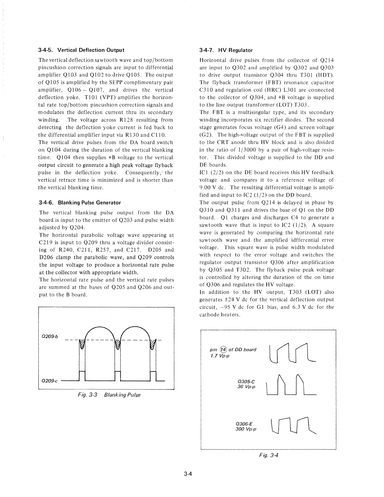
3-4-6. Blanking
Pulse
Generator
The
vertical blanking pulse
output
from
the
DA
board
is
input
to
the
emitter
of
Q203
and
pulse
width
adjusted
by
Q204.
The
horizontal
parabolic voltage wave appearing
at
C219
is
input
to
Q209
thru
a voltage divider consist-
ing
of
R240,
C211,
R257,
and C217. D205
and
D206
clamp
the
parabolic
wave,
and
Q209
controls
the
input
voltage
to
produce
a
horizontal
rate
pulse
at
the
collector
with
appropriate
width.
The
horizontal
rate pulse
and
the
vertical
rate
pulses
are
summed
at
the
bases
of
Q205
and
Q206
and
out-
put
to
the
B
board.
0209-b
0209-c
Fig.3-3
Blanking Pulse
3-4
3-4-7.
HV
Regulator
Horizontal
drive pulses from
the
collector
of
Q214
are
input
to
Q302
and
amplified by
Q302
and Q303
to
drive
output
transistor Q304
thru
T301 (HDT).
The
flyback
transformer
(FBT) resonance
capacitor
C310
and regulation coil (HRC) L30 I are
connected
to
the
collector
of
Q304,
and
+B
voltage
is
supplied
to
the
line
output
transformer
(LOT)
T303.
The
FBT
is
a multisingular
type,
and
its
secondary
winding
incorporates
six rectifier diodes. The
second
stage generates focus voltage
(G4)
and screen voltage
(G2). The high-voltage
output
of
the
FBT
is
supplied
to
the
CRT
anode
thru
HV
block
and
is
also divided
in
the
ratio
of
1/3000
by a pair
of
high-voltage resis-
tor.
This divided voltage
is
supplied
to
the
DD and
DE boards.
IC I
(2/2)
on
the
DE board receives this HV feedback
voltage
and
compares it
to
a reference voltage
of
9.00
V dc.
The
resulting differential voltage
is
ampli-
fied
and
input
to
IC2
(1/2)
on
the
DD board.
The
output
pulse from
Q214
is
delayed in phase by
Q310
and
Q311
and
drives
the
base
of
Q I
on
the
DD
board. Q I charges and discharges C4
to
generate
a
sawtooth
wave
that
is
input
to
IC2
(1/2).
A square
wave is
generated
by comparing
the
horizontal
rate
sawtooth
wave
and
the
amplified idfferential error
voltage. This
square
wave
is
pulse
width
modulated
with respect
to
the
error
voltage
and
switches
the
regulator
output
transistor
Q306
after
amplification
by Q305
and
T302.
The fly back pulse peak voltage
is
controlled
by altering the
duration
of
the
on
time
of
Q306
and
regulates
the
HV voltage.
In
addition
to
the
HV
output,
T303
(LOT)
also
generates ±24 V dc for
the
vertical deflection
output
circuit,
-95
V dc for
GI
bias,
and
6.3 V dc for the
cathode
heaters.
pin
@
of
DD
board
1.7
Vp-p
0305-C
36
Vp-p
0306-E
300
Vp-p
Fig. 3-4