2-2.
CIRCUIT BOARDS LOCATION
Note: The components identified by shading and mark
til
are critical for safety. Replace only with
part number specified.
f«~rn.;;;-x~r
:~:~;-:·:~~\;::~:~~~~t.:i:;~mm:U~;~~~~J.L~;
':'
...
_
.:,~
...
;~;~~-:;~J.:;:;;~~~
tt
Nota:
Las
compossnts idantifi6s par una trame
at
~
0!
Plr
une marque
til
sont
d'una
importance
~
~~
. critique
pour
II. s6curit6.
Ne
les
ramp.l~cer
m
#'
aue
par des pulces
de
num6ro sp6clfl6.
~
~k~~t!~::~J~:~~J~~~i~ti;~?k~U~t.W.;~:;:
-~::)'-~;
.)){rr~0.~~~~
Not.:
•
All
capacitors
are in /IF unless
otherwise
noted.
p : /l/lF 50WV
or
less are
not
indicated
except
for
electrolytics.
• All resistors are in
ohms,
I/SW unless
otherwise
noted.
k :
1000n,
M :
1000kn.
•
-e-
:
nonflammable
resitor.
• All variable
and
adjustab
le resistors have
characteristic
curve B,
unless
otherwise
noted.
•
~
: fusible resitor.
• a : internal
component.
•
c=J:
panel
designation.
•
if
: selected
to
yield
optimum
performance
.
•
The
components
indentifled
by
B in this manual have been
carefully
factory·selacted
for each sat in
order
to
satisfy
reo
gulations regarding X·ray radiation.
Should
replacement
be
required,
replace
only
with
the
value originally
used.
• When replacing
components
identified
by
(;iii
mark
the
neces·
sary
adjustments
indicated
.
If
results
do
not
meet
the
specified
value, change
the
component
i
dentified
by
B
and
repeat
the
adjustment
until
the
specified value
IS
achieved.
(Refer
to
R339,
R41S, R489 adjUStment
on
page
II,
12.1
When replacing
the
part
in
below
table,
be
usre
to
perform
the
related
adjustment
.
Pan
,.pl.eld
I tii )
Ad,uumlnl
I
Y}
IG
Baardl D6SJ, R65B. R659.
T65J
t
SA
BOlrdl
IC401, IC404, IC405, Q409, R409. R410.
R4",
R416, R4B9
R412, R41J, R414, R415, A416, A417. A41B"
I.B
MAXI
A419, A424. R425, R448, A479,
A4BO,
A4BB,
A4B9
,
IBA
Balrdl
1C301, ICJ02,
AlOl,
Rl02,
AJJ5,
RJJ6,
RJJ7,
AJl9
AllB.
AlJ9,
AJ40. AJ41.
AJ42,
OJ04
IHV
HOLD
OOWNI
10 Baardl A565, A568
• Voltages are
de
with
respect
to
ground
unless
otherwise
noted.
• Readings
are
taken
with
a
10
Mn
digital
multlmeter
.
• Voltage variations
my
be
noted
due
to
normal
production
tolerances.
• Readings are
taken
with a color-bar signal
Input
.
(MU
L TI
SCAN
GENERATOR
JIGI
•
c=J:
adj
ustment
to
repair.
• no mark:
with
15.7SkHz
(SOHz
VI
color-bar signal received.
(
I: wi
th
31
.52kHz (70Hz
VI
color-bar signal received.
MULTI SCAN GENERATOR
JIG
VR POSITION
FREO
I
POSITION
Al-
I
(V
1
-::-
NORMAL
MODE
1576kHz
A B
160HzI
A B
2 1 3
7
F
2H
MODE
3152kHz
9
1
2 2 5
170Hzl
I
A
B
c
o
E
F
G
H
J
n
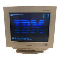
CPD-1302
CPD-1302
2-3.
SCHEMATIC DIAGRAMS
1 2
Be
~;:;~
Ec
•
~O.4~
,
~
..
L9OIio.~
i
ec
-
2
BA
Board IC201 BLOCK
DIAGRAM
CXA1044P
(VIDEO
AMP)
::- -
}~'"
-
.J
a
SA-
3
BA(
HV
ose,
R
·G·
B
DRIVE.
)
V.
FREQ
CTRT,
FIV
CONV.
I V
..
I
V
•
'li8'
I
~
4
5
6
7
8
9
10
11
.--{TO
H-~
I BA-3 , I
BA-12
;f
~
,
BA
' 14
..
~
,.
"
....
12
Q440
OTCI44E5
11
111
" I
~~:"
'f;V"
....
l .U
It l
....
l
1
13
..c
~
!--t=:t=::t==
"4
10
",
-
lL!<....I!l!r.l - - , - I
HPBIAS
I
,,,,
llk.O!!llJ
..
I
'"
~
"'"-
...
"'
!O
.- ,"
UtS~2f8~5b
i'f.·
'11~
~
'12
m
,
"I
0293
2SC2785
0294
2SA1I75
'''1i:JlJ
[i
:
I)"'1
t
'§:
~;ll'
=Y"
'IT.
".
!\\!"l;®l'
ITl,'
00.
~FF
"
oJ
~""
"
""
...
..
~
'""""'""
~!'I~
~
':W'"
p:Jc'....
""
"
,.
~
IIl
f
!
~
~
I
.-
0255
256
~'""'"I
-
-++-
-
+-+'=::-==:-:,:,:-
....,~-:
=::-===:----:-:-::!
..
0 I
..
,--"~-
f&Q4
11
~
m;,,~
'
~P~=~~~::::;.;;;-id
=~
-
~
OI
~
·
V
""'~E
~~~~~;
-f'~
·
~'
1
"
~"'~
21
155il9 0402
R06.8E-N2
i!lJ
IC
401
NJM4SS85
0412
414 258740 " " I'
'"
""
1'10 -
~
-
,
,_
~
"'
02942SAI175
~
u
~~~
t
~~~~~=~~_~
~
_
'
_~~P
_
~
_
~
_
Z
1
~
~
I
~
__
~~~_
I
V
_
m
_
B
~
.
~
F
i
l
~_~~;~
'
I
~
'H
~
n
;
I
~~~
~!
:
!
U
~
'
~
~~g
~~~~~
~
~
t
~~
~
~
'
~~
'
~
Ol
g~!~
~
0297
25C2785
,m I
~'"
rf,
"1:'
"
r-
"."
0413
2SC2785
0415
25C2785
':Jl
0"
~
~~"I
""
~f
1il:
""
,,,.
IRlli!Il • ...
""'"1-l.J
...
.
...,....IP-·-.-Iti~''''1l',.....t+-t++-!-+--+-'
~
~
r;;1
\
~
:~'
...
ffi'
[
~
,r-err
It'"
~''0401
0404 0405 0407
0321
0322
'1'
0291,292
2SA1I75
e",
~r.
'
llliW
I
.:;;~
,
t~
It'"
25AII75
2SC2785
2SAII75
25AII75
2SC2785
25C2785
~lt'
W
~~
I
CRN
TMI
.R
-I
.21
-01
I
...
,'
" , ,P,
-;;;;
lt~
r
!'~l'
~
'~:
I
;r,
j':;"
!
VCC
O
"
4
J11
~;
- "
~
~
~
~
3,32
~
~Ol!l'
~
.
'itt 0
0313
<
..
~
[Do I J I
~
IC,.,
2
~
=
~
"
I
i:
~
,.".
Q252
25A!l75
..
"..
25C2785
2~:fth
2SC2785
25C2785
2SC2785
...
~I
~
)GI<
IC205
5N74LS22IN
~
..
~
2
~ ~
5
~
M
:'j.I
r
'It'
urnm
~:::.~
~
~
IillJJMiEJ
~
~!IT8fI:IiI
I
~
~'
..
,.!. -
~
'
~
0325,.
!iiJiiitll
~
.
"1
'
• T 011
...
4
TcJ
ti
,:
:r
""
""I""
0254
155119
~
J
~
ur
'"
~
I~I
~
"
-i.l
',
1.!'
"'"
IT' _
BA-17
~
________________________________
____
__________
__
____________
--'~T~O~~:2~2~===~::=r-
__
IB
_
~
_1
5
____
-C~~~~~J~J~~~~
B~
C
9
~roc~~
tt±:j--
·,A
-
-
-
'
----------------------------------
________
~~~~~ttt±j--~-
-
-
"
--------------------
---
-
TO
CA
TO
'-3)--
:..-
0-
1('\