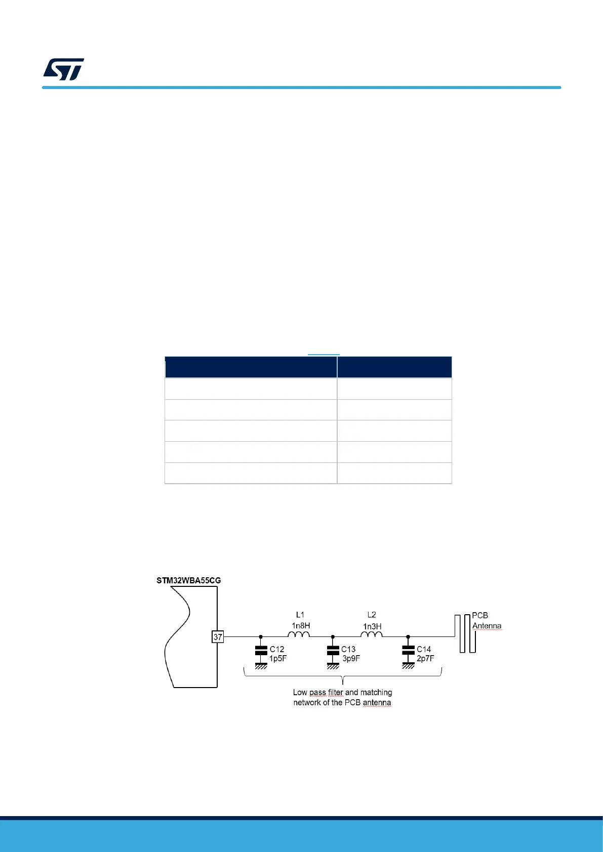
6.5 RF I/O stage
Due to FCC/ISED constraints, the antenna cannot be removable. So, the board is proposed by default with a
PCB antenna. This antenna is described on AN5129 available on the ST web site. Between the
STM32WBA55 and the antenna, there is a passive network. This network has got two functions: makes a low
pass filter and matches the impedance of the PCB antenna. These both functions are merged to reduce the
number of components.
The output stage of the STM32WBA55 was optimized for this impedance of 50 ohms. That allow to facilitate
the design of the external part.
Therefore, the low pass filter was study with an impedance of 50 ohms for SoC side and with the antenna
impedance for the other side. To simplify, the bandwidth of the antenna was not taken in count. Parts of
harmonics are filtered internally but for silicone size and cost, they are not completely suppressed. The low
pass filter is to reduce the level of the harmonic to satisfy the certifications requirements (FCC, ISED, RED,
MIC,…).
The table 8 shows the level of harmonic expected worst case at the output of the STM32WBA55 without filter.
That allows to determinate the attenuation of the filter vs. frequency.
Table 8. harmonic level on the STM32WBA55 without external filter (TX mode@+10dBm)
This network is built with 5 components C12, L1, C13, L2, and C14. That guaranteed a comfortable margin in
all cases. The study takes in count, the drift of the components (accuracy and temperature), the drift due to
the PCB, and the variation of the STM32WBA55. Of course, depending on the components manufacturer and
the specification of the PCB, these components values can change after mandatory optimisation.
Figure 4 RF I/O stage