EasyManuals Logo

ST STM32 NUCLEO-F411RE User Manual

ST STM32 NUCLEO-F411RE
68 pages
To Next Page IconTo Next Page
To Previous Page IconTo Previous Page
Page #19 background imageLoading...
Page #19 background image
UM1724 Rev 14 19/68
UM1724 Hardware layout and configuration
67
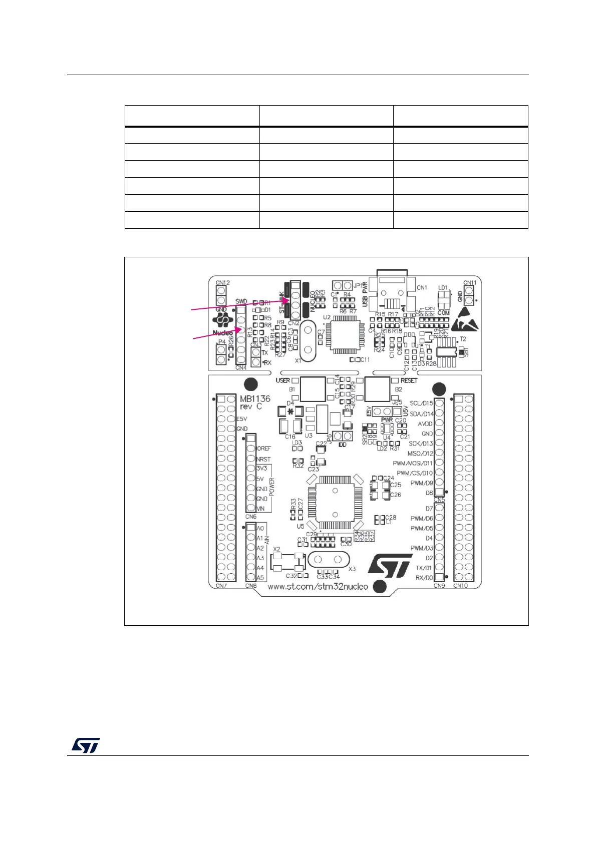
Figure 9. Using ST-LINK/V2-1 to program the STM32 on an external application
Table 5. Debug connector CN4 (SWD)
Pin CN4 Designation
1 VDD_TARGET VDD from application
2 SWCLK SWD clock
3 GND ground
4 SWDIO SWD data input/output
5 NRST RESET of target STM32
6 SWO Reserved
MS34379V2
CN2 jumpers OFF
CN4
SWD connector

Table of Contents

Questions and Answers:

Question and Answer IconNeed help?

Do you have a question about the ST STM32 NUCLEO-F411RE and is the answer not in the manual?

ST STM32 NUCLEO-F411RE Specifications

General IconGeneral
MicrocontrollerSTM32F411RET6
CoreARM Cortex-M4
Operating Voltage3.3V
Input Voltage7V to 12V
Operating Frequency100 MHz
Flash Memory512 KB
SRAM128 KB
Digital I/O Pins50
Analog Input Channels16
DAC Channels1
On-board DebuggingST-LINK/V2-1
Communication InterfacesI2C, SPI, USART
USBUSB 2.0
ConnectorsArduino Uno
Form FactorNucleo

Related product manuals