EasyManua.ls Logo

ST STM32F401 User Manual

ST STM32F401
38 pages
To Next Page IconTo Next Page
To Previous Page IconTo Previous Page
Page #14 background image
Hardware layout UM1669
14/39 DocID025174 Rev 1
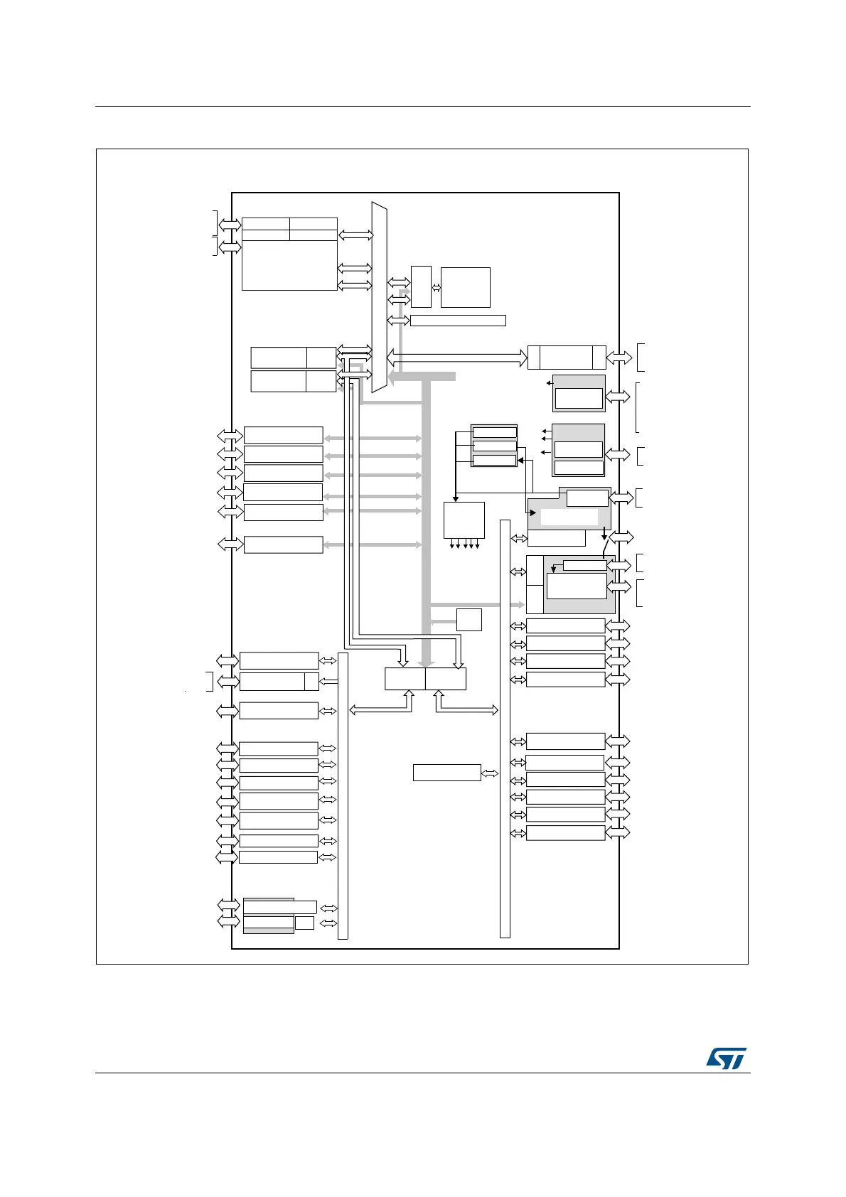
Figure 5. STM32F401VCT6 block diagram
GPIO PORT A
AHB/APB2
EXT IT. WKUP
up to 81 AF
PA[15:0]
TIM1 / PWM
4 compl. channels TIM1_CH1[1:4]N,
4 channels TIM1_CH1[1:4]ETR,
BKIN as AF
USART1
RX, TX, CK,
CTS, RTS as AF
SPI1
MOSI, MISO,
SCK, NSS as AF
APB2 60MHz
APB1 30MHz
16 analog inputs
VDDREF_ADC
MOSI/SD, MISO/SD_ext, SCK/CK
NSS/WS, MCK as AF
SP3/I2S3
ALARM_OUT
OSC32_IN
OSC32_OUT
VDDA, VSSA
NRST
smcard
irDA
16b
VBAT = 1.65 to 3.6 V
DMA2
SCL, SDA, SMBA as AF
I2C3/SMBUS
JTAG & SW
ARM Cortex-M4
84 MHz
NVIC
ETM
MPU
TRACECLK
TRACED[3:0]
DMA2
8 Streams
FIFO
ACCEL/
CACHE
AHB1 84 MHz
USART 2MBps
Temperature sensor
ADC1
IF
@VDDA
POR/PDR
BOR
Supply
supervision
@VDDA
PVD
Int
POR
reset
XTAL 32 kHz
MANAGT
RTC
RC HS
RC LS
PWR
interface
WDG 32K
@V
BAT
@VDDA
@VDD
AWU
Reset &
clock
control
PLL1&2
APB2CLK
VDD = 1.7 to 3.6 V
VSS
VCAP
Voltage
regulator
3.3 to 1.2 V
VDD
Power managmt
@VDD
STAMP1
Backup register
AHB bus-matrix 7S4M
APB2 84 MHz
LS
TIM9
2 channels as AF
Flash
up to
256 KB
TIM2
TIM3
TIM4
TIM5
D-BUS
MS31144V2
FPU
APB1 42 MHz (max)
AHB2 84 MHz
NJTRST, JTDI,
JTCK/SWCLK
JTDO/SWD, JTDO
I-BUS
S-BUS
DMA1
8 Streams
FIFO
PB[15:0]
PC[15:0]
PH[1:0]
GPIO PORT B
GPIO PORT C
GPIO PORT H
16b
TIM10
16b
TIM11
16b
smcard
irDA
USART6
1 channel as AF
1 channel as AF
RX, TX, CK as AF
I2C2/SMBUS
I2C1/SMBUS
SCL, SDA, SMBA as AF
SP2/I2S2
MOSI/SD, MISO/SD_ext, SCK/CK
NSS/WS, MCK as AF
RX, TX as AF
CTS, RTS as AF
USART2
smcard
irDA
32b
16b
16b
32b
4 channels
4 channels, ETR as AF
DMA1
AHB/APB1
LS
OSC_IN
OSC_OUT
HCLK
XTAL OSC
4- 16MHz
SRAM 64 KB
WWDG
APB1CLK
AHB1PCLK
AHB2PCLK
CRC
(PDR OFF)
1.8 to 3.6 V
(PDR ON)
SDIO / MMC
FIFO
D[7:0]
CMD, CK as AF
USB
OTG FS
FIFO
PHY
DP
DM
ID, VBUS, SOF
SPI4
MOSI, MISO,
SCK, NSS as AF
PD[15:0]
GPIO PORT D
PE[15:0]
GPIO PORT E
Question and Answer IconNeed help?

Do you have a question about the ST STM32F401 and is the answer not in the manual?

ST STM32F401 Specifications

General IconGeneral
SeriesSTM32F4
CoreARM Cortex-M4
Clock Speed84 MHz
Communication InterfacesI2C, SPI, USART, USB
Operating Voltage1.7 V to 3.6 V
Number of I2Cs3
Number of SPIs3
Number of USARTs3
ADC12-bit
DAC12-bit
TimersAdvanced-control timers
Operating Temperature Range-40°C to 85°C
PackageLQFP64, LQFP48

Summary

Introduction

STM32F401 Discovery Kit Overview

Introduces the STM32F401 Discovery kit for evaluating and developing STM32F4 applications.

Conventions

Document Conventions and Definitions

Explains conventions for jumpers, solder bridges, and other symbols used in the manual.

Quick start

Getting Started with STM32F401 Discovery Kit

Step-by-step guide to configure and launch the DISCOVER application on the STM32F401 board.

STM32F401 Discovery Kit System Requirements

Lists necessary PC, OS, and USB cable requirements for using the STM32F401 Discovery kit.

Development Toolchains for STM32F401 Discovery Kit

Identifies compatible IDEs and toolchains for developing applications with the STM32F401 Discovery kit.

STM32F401 Discovery Kit Order Code

Provides the official order code for purchasing the STM32F401 Discovery kit.

Features

Key Features of the STM32F401 Discovery Board

Details the core features and benefits of the STM32F401 Discovery board, including MCU, sensors, and connectivity.

Hardware layout

STM32F401VCT6 Microcontroller Details

Details the STM32F401VCT6 microcontroller's specifications, performance, and power efficiency benefits.

Embedded ST-LINK/V2 for Programming

Explains the integrated ST-LINK/V2 for programming and debugging the STM32F401 on-board.

Using ST-LINK/V2 for On-Board STM32F401 Programming

Instructions for utilizing the onboard ST-LINK/V2 to program the STM32F401 microcontroller.

Using ST-LINK/V2 for External STM32 Application Debugging

Guide for using the board's ST-LINK/V2 to program an external STM32 application board via CN2.

Power Supply and Selection Options

Describes how the board receives power and the available selection options for power sources.

Board LEDs and Indicators

Details the function and location of all LEDs on the STM32F401 Discovery board.

User and Reset Pushbutton Functions

Explains the function of the user (B1) and reset (B2) pushbuttons on the board.

On-Board Audio Circuitry

Describes the audio DAC, MEMS microphone, and audio output capabilities of the board.

USB OTG Support and Status LEDs

Details the USB OTG full speed functionality and its associated status LEDs (LD7, LD8).

E-compass MEMS Sensor (LSM303DLHC)

Describes the E-compass MEMS sensor (LSM303DLHC) and its 3D acceleration/magnetic measurement capabilities.

Gyroscope MEMS Sensor (L3GD20)

Describes the Gyroscope MEMS sensor (L3GD20) and its three-axis angular rate measurement capabilities.

JP2 Jumper for Current Measurement

Explains the JP2 jumper's role in measuring the STM32F401VCT6's current consumption.

Oscillator Clock Supply Configurations

Details configurations for various oscillator clock supply sources and the 32 KHz clock.

Solder Bridge Configurations and Functions

Describes the function and states of various solder bridges for board configuration.

Extension Connector Pinouts and Usage

Details the male headers P1 and P2 for connecting to external prototyping boards and probing.

Mechanical drawing

STM32F401 Discovery Board Mechanical Diagram

Provides a detailed mechanical drawing of the STM32F401 Discovery board with key dimensions and component placement.

Electrical schematics

STM32F401 Discovery Board Overall Schematics

Presents the main electrical schematic diagram for the STM32F401 Discovery board.

ST-LINK/V2 Interface Schematics

Electrical schematic detailing the ST-LINK/V2 programming and debugging interface.

STM32F401VCT6 Microcontroller Schematics

Schematic diagram showing the connections and configuration of the STM32F401VCT6 microcontroller.

Audio Circuitry Schematics

Electrical schematic for the board's audio DAC, MEMS microphone, and audio output components.

USB OTG Full Speed Schematics

Electrical schematic detailing the USB OTG Full Speed interface and associated components.

Peripherals Schematics (MEMS, Buttons, LEDs)

Electrical schematics for the board's MEMS sensors, pushbuttons, and LEDs.

Revision history

Document Revision History

Records the revision history and changes made to this document over its lifecycle.

Related product manuals