DocID025174 Rev 1 21/39
UM1669 Hardware layout
37
Oscillator from external PC14 (from external oscillator trough the pin 9 of P2 connector)
The configuration needed is:
– SB17closed
– SB18 closed
– R21 and R22 removed
4.12 Solder bridges
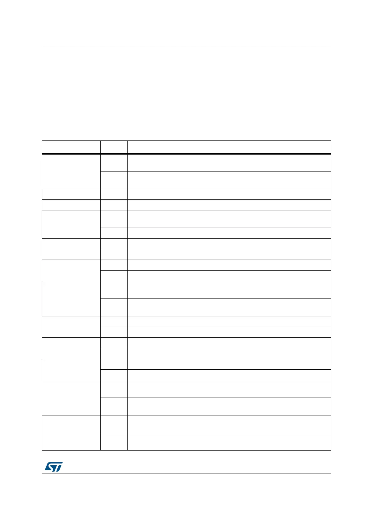
Table 5. Solder bridges
Bridge State
(1)
Description
SB14,16 (X2 crystal)
OFF
X2, C18, C19, R24 and R25 provide a clock.
PH0, PH1 are disconnected from P2
ON
PH0, PH1 are connected to P2
R24, R25 and R66 must not be fitted).
SB3,5,7,9 (Default) ON Reserved, do not modify
SB2,4,6,8 (Reserved) OFF Reserved, do not modify
SB17,18 (X3 crystal)
OFF
X3, C20, C28, R21 and R22 deliver a 32 KHz clock.
PC14, PC15 are not connected to P2.
ON PC14, PC15 are only connected to P2. Remove only R21, R22
SB1 (B2-RESET)
ON B2 pushbutton is connected to the NRST pin of the STM32F401VCT6 MCU
OFF B2 pushbutton is not connected to the NRST pin of the STM32F401VCT6 MCU
SB21 (B1-USER)
ON B1 pushbutton is connected to PA0
OFF B1 pushbutton is not connected to PA0
SB13 (NRST)
ON
NRST signal of the CN2 connector is connected to the NRST pin of the
STM32F401VCT6 MCU
OFF
NRST signal of the CN2 connector is not connected to the NRST pin of the
STM32F401VCT6 MCU
SB15 (SWO)
ON SWO signal of the CN2 connector is connected to PB3
OFF SWO signal is not connected
SB10,11 (RX,TX)
OFF Reserved, do not modify
ON Reserved, do not modify
SB12 (STM_RST)
OFF No incidence on STM32F103C8T6 (ST-LINK/V2) NRST signal
ON STM32F103C8T6 (ST-LINK/V2) NRST signal is connected to GND
SB19 (BOOT0)
ON
BOOT0 signal of the STM32F401VCT6 MCU is held low through a 510
Ω pull-
down resistor
OFF
BOOT0 signal of the STM32F401VCT6 MCU is held high through a 10 K
Ω pull-
up resistor
SB20 (BOOT1)
OFF
The BOOT1 signal of the STM32F401VCT6 MCU is held high through a 10 K
Ω
pull-up resistor
ON
The BOOT1 signal of the STM32F401VCT6 MCU is held low through a 510
Ω
pull-down resistor