8 STM32G0 Nucleo-32 I/O assignment
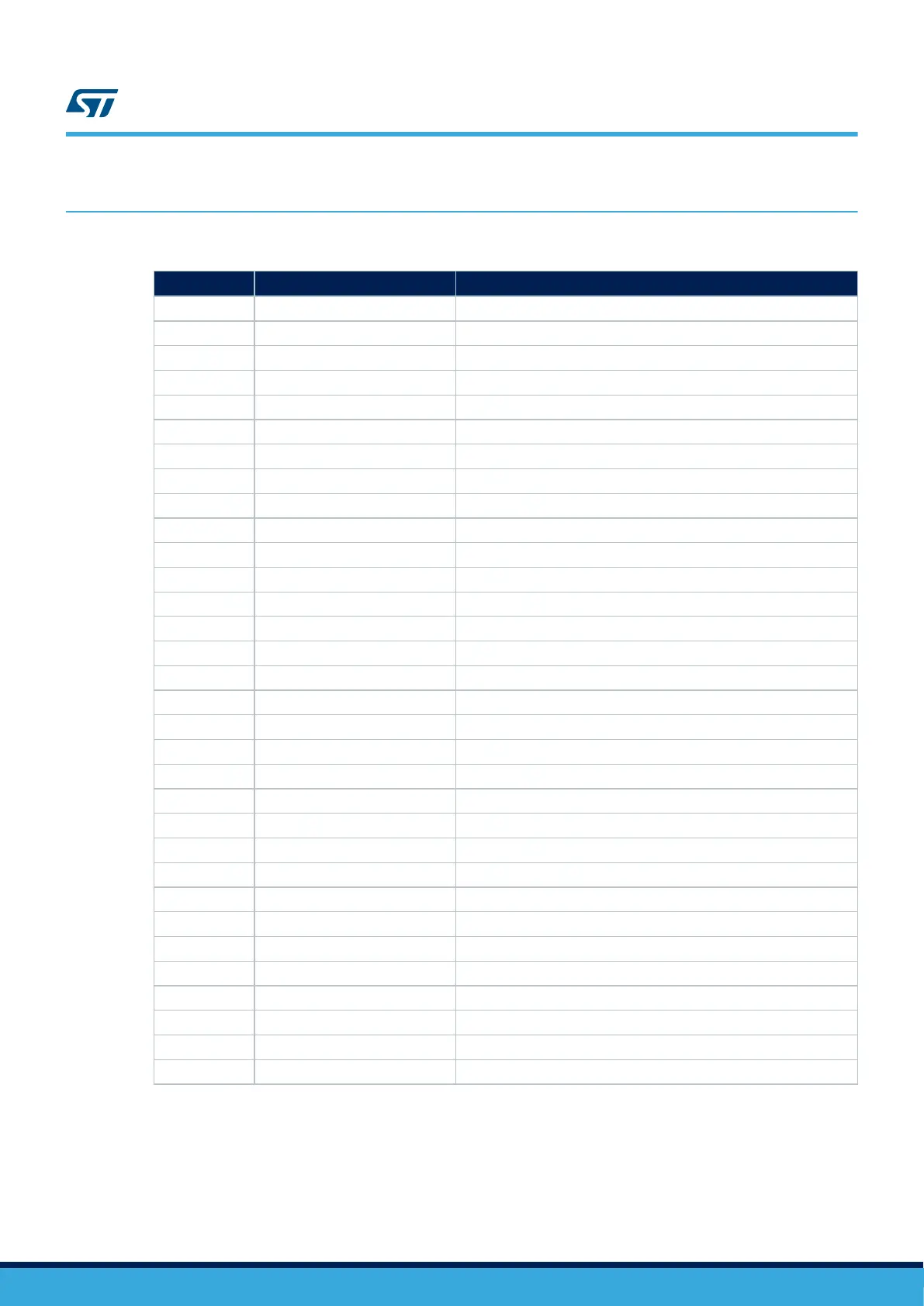
Table 10. Nucleo-32 I/O assignment
Pin Pin name Main feature / optional feature
1 PB9 ARD_D10: SPI1_CS(2) / TIM1_CH4
2 PC14-OSC32_IN LSE clock input
3 PC15-OSC32_OUT LSE clock output
4 VDD VDD voltage supply
5 VSS Ground ARD_A4: DC2_IN13
6 PF2-NRST RESET – USER button
7 PA0 ARD_A0: ADC_IN0
8 PA1 ARD_A1: ADC_IN1
9 PA2 VCP_TX: USART1_Tx
10 PA3 VCP_RX: USART1_Rx
11 PA4 ARD_A2: ADC_IN4
12 PA5 ARD_A3: ADC_IN5
13 PA6 ARD_A6: ADC_IN6
14 PA7 ARD_A7: ADC_IN7
15 PB0 ARD_D6: PWM: TIM3_CH2
16 PB1 ARD_D3 - PWM: TIM3_CH4
17 PB2 ARD_D7: I/O
18 PA8 ARD_D9: PWM: TIM1_CH1
19 PA9 ARD_D5: TIM1_CH2 / I2C1_SCL
20 PC6 USER LED
21 PA10 ARD_D4: TIM1_CH3 / I2C1_SDA
22 PA11 [PA9] ARD_A5: ADC_IN15 / I2C2_SCL
23 PA12 [PA10] ARD_A4: ADC_IN16 / I2C2_SDA
24 PA13 SWDIO
25 PA14-BOOT0 SWCLK
26 PA15 ARD_D2: I/O
27 PB3 ARD_D13: SPI1_SCK
28 PB4 ARD_D12: SPI1_MISO
29 PB5 ARD_D11: SPI1_MOSI / TIM3_CH2
30 PB6 ARD_D0: USART1_RX
31 PB7 ARD_D1: USART1_TX
32 PB8 ARD_D8: I/O
UM2591
STM32G0 Nucleo-32 I/O assignment
UM2591 - Rev 1
page 18/26