DocID029918 Rev 1 23/48
AN4938 Boot configuration
47
4 Boot configuration
4.1 Boot mode selection
In STM32H743/753xx microcontrollers, two different boot spaces can be selected through
the BOOT pin and the boot base address programmed in the BOOT_ADD0 or BOOT_ADD1
option bytes as shown in the
Table 1.
The BOOT_ADD0 and BOOT_ADD1 address option bytes allow to program any boot
memory address from 0x0000
0000 to 0x3FFF 0000 which include:
• All the Flash memory address space mapped on AXIM interface.
• All the RAM address space: ITCM, DTCM RAMs and SRAMs mapped on AXIM
interface.
• The system memory bootloader.
The BOOT_ADD0/BOOT_ADD1 option bytes can be modified after the reset in order to
boot from any other boot address after the next reset.
If the programmed boot memory address is out of the memory mapped area or a reserved
area, the default boot fetch address is programmed as follows:
• Boot address 0: Flash memory at 0x0800 0000
• Boot address 1: ITCM-RAM at 0x0000 0000
When the Flash level 2 protection is enabled, only boot from Flash memory is available. If
the boot address already programmed in the BOOT_ADD0 / BOOT_ADD1 option bytes is
out of the memory range or belongs to the RAM address range, the default fetch will be
forced from Flash memory at address 0x0800 0000.
Note: When the Secure access mode is enabled through option bytes, the boot behavior differs
from the above description (refer to section Root secure services of the product reference
manual).
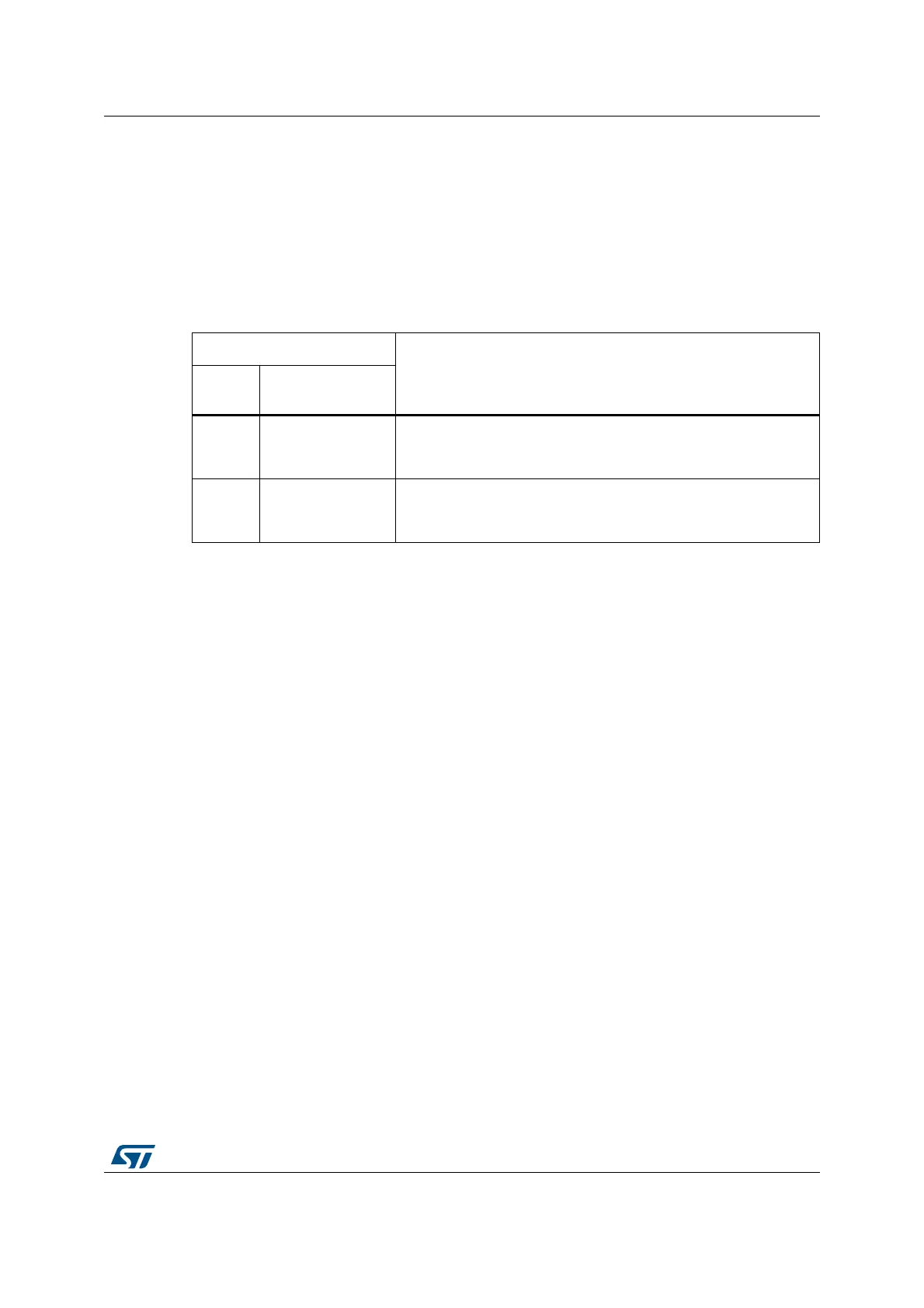
Table 1. Boot modes
Boot mode selection
Boot space
BOOT
pin
Boot address
option bytes
0 BOOT_ADD0 [15:0]
Boot address defined by BOOT_ADD0[15:0] user option byte
Default factory programmed value: User Flash memory starting at
0x0800 0000
1 BOOT_ADD1 [15:0]
Boot address defined by BOOT_ADD1[15:0] user option byte
Default factory programmed value: System Flash memory starting
at 0x1FF0 0000

 Loading...


