DocID029918 Rev 1 33/48
AN4938 Reference design
47
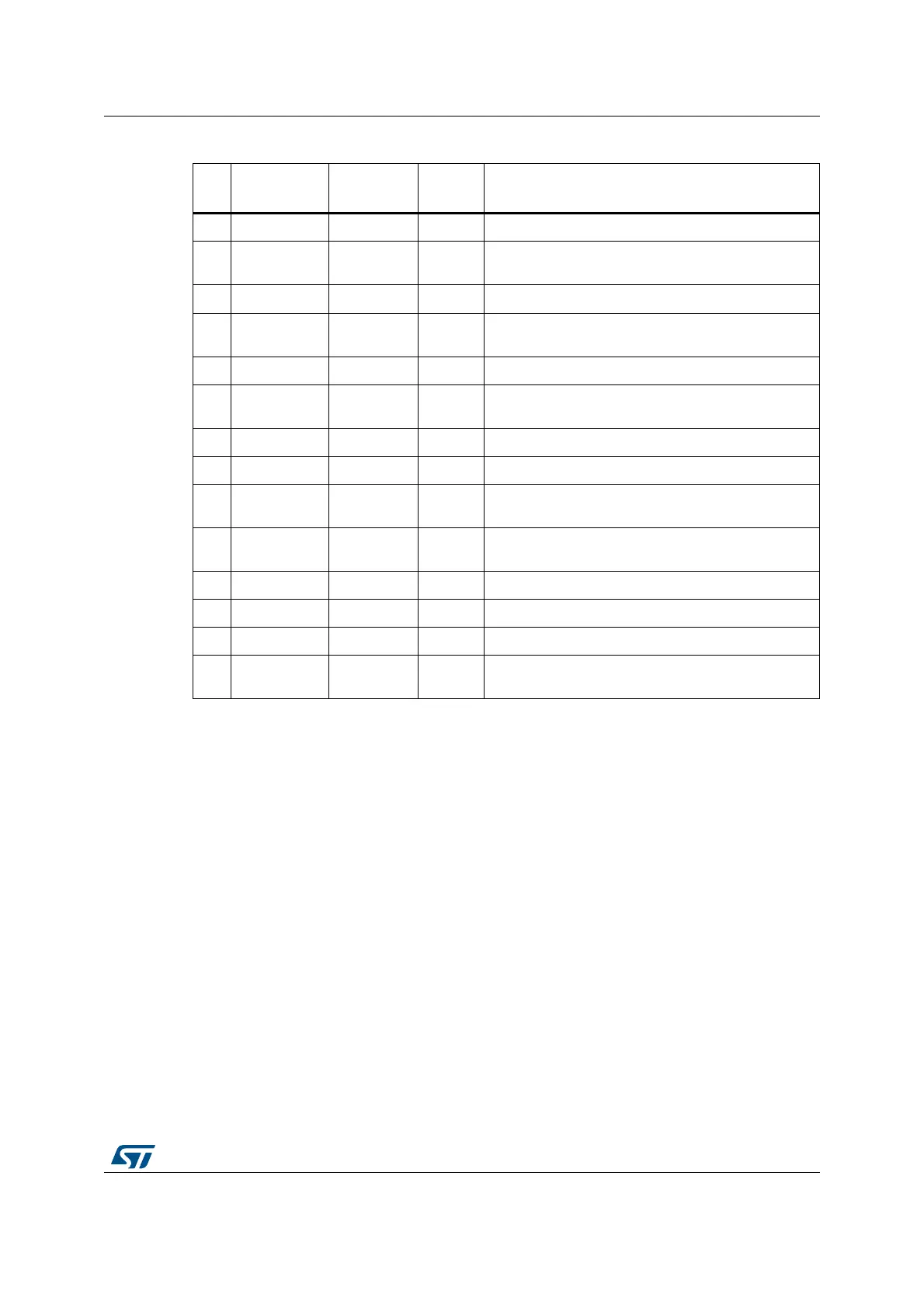
Table 8. Optional components
Id
Components
name
Reference Quantity Comments
1
Resistor 10 kΩ 5 Pull-up and pull-down for JTAG, BOOT pin, PDR
2
Resistor 0 Ω 1
Used as star connection point between V
DDA
and
V
REF+
3
Capacitor 100 nF 3 Ceramic capacitor
4
Capacitor 1.5 pF 2
Used for LSE: the value depends on the crystal
characteristics
5
Capacitor 1 μF 3 Used for V
DDA
, V
REF
and V
DDUSB
6
Capacitor 3.9 pF 2
Used for HSE: the value depends on the crystal
characteristics
7
Quartz 25 MHz 1 Used for HSE
8
Quartz 32.768 kHz 1 Used for LSE
9
JTAG
connector
HE10-20 1 –
10
Battery 3 V 1
If no external battery is used in the application, it is
recommended to connect V
BAT
externally to V
DD
.
11
Switch SPDT 1 Used to select the right boot mode.
12
Push-button B1 1 Reset button
13
Jumper 3 pins 2 Used to select V
BAT
source
14
Ferrite bead
FCM1608KF
-601T03
1 Additional decoupling for V
DDA
 Loading...


