Recommended PCB routing guidelines for STM32H743/753xx devices AN4938
40/48 DocID029918 Rev 1
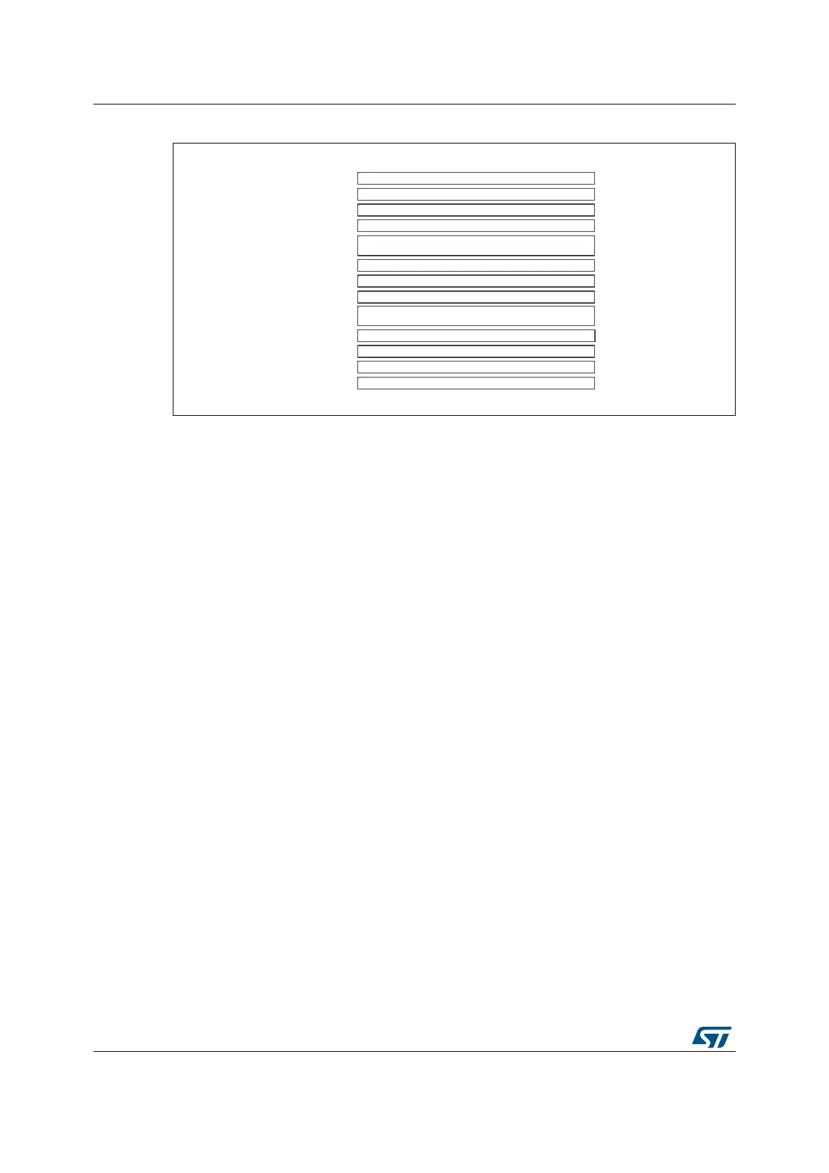
Figure 21. Six layer PCB stack-up example
8.2 Crystal oscillator
Use the application note: Oscillator design guide for STM8S, STM8A and STM32
microcontrollers (AN2867), for further guidance on how to layout and route crystal oscillator
circuits.
8.3 Power supply decoupling
An adequate power decoupling for STM32H743/753xx devices is necessary to prevent an
excessive power noise and ground bounce noise. Please refer to
Section 1.2: Power supply
scheme.
The following recommendations shall be followed:
• Place the decoupling capacitors as close as possible to the power and ground pins of
the MCU. For BGA packages, it is recommended to place the decoupling capacitors on
the other side of the PCB (see
Figure 22).
• Add the recommended decoupling capacitors for as many V
DD
/GND pairs as possible.
• Connect the decoupling capacitor pad to the power and ground plane with a wider,
short trace/via. This allows reducing the series inductance, maximizing the current flow
and minimizing the transient voltage drops from the power plane which also reduces
the possibility of ground bounce.
Figure 23 shows an example of decoupling capacitor placement underneath
STM32H743/753xx devices, closer to the pins and with less vias.
06Y9
6ROGHU0DVN
+LJK6SHHG6LJQDOV*1'
*1'3ODQH
3RZHU3ODQH
+LJK6SHHG6LJQDOV*1'
3UHSHJ
&RUH
3UHSHJ
6ROGHU0DVN
/D\HUB7RS
/D\HUB,QQHU
/D\HUB,QQHU
/D\HUB%RWWRP
3UHSHJ
/RZ6SHHG6LJQDOV
&RUH
*1'3ODQH
/D\HUB,QQHU
/D\HUB,QQHU
 Loading...


