Depending on the STM32 device, additional protections are available, including:
• backup registers for real-time clock (RTC)
• backup SRAM
• Nonvolatile memories
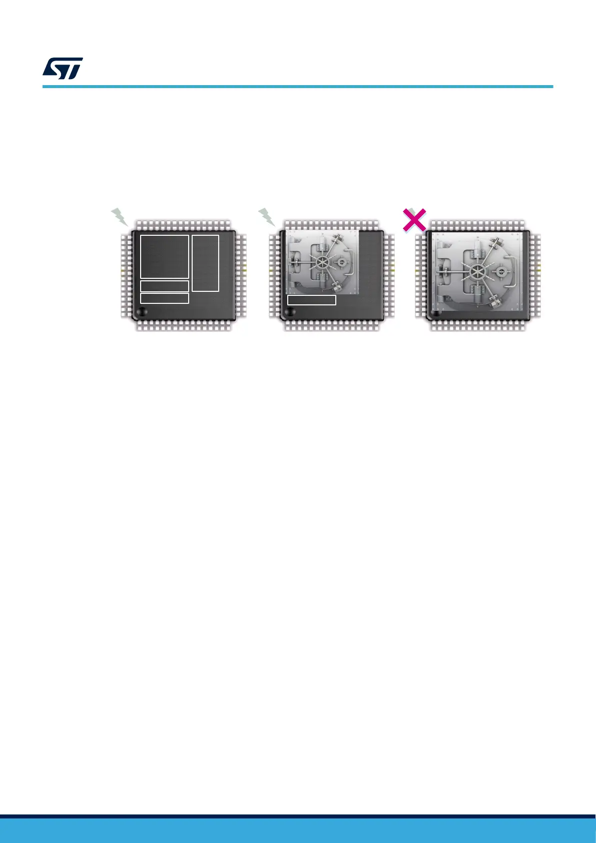
Figure 8. Example of RDP protections (STM32L4 series)
DT50952V1
SRAM1
FLASH
SRAM
Backup
Reg
Level 0
SRAM2
FLASH
SRAM1
Backup
registers
SRAM
FLASH
SRAM
Backup
Reg
Level 1 Level 2
Debug port
The RDP levels are defined as follows:
• Level 0(default RDP level)
The flash memory is fully open, and all memory operations are possible in all boot configurations (debug
features, boot from RAM, boot from system memory bootloader, boot from flash memory). There is no
protection in this configuration mode that is appropriate only for development and debug.
• Level 1
Flash memory accesses (read, erase, program), or SRAM2 accesses via debug features (such as serial-
wire or JTAG) are forbidden, even while booting from SRAM or system memory bootloader. In these cases,
any read request to the protected region generates a bus error.
However, when booting from flash memory, accesses to both flash memory and to SRAM2 (from user
code) are allowed.
• Level 2
All protections provided in Level 1 are active, and the MCU is fully protected. The RDP option byte and all
other option bytes are frozen, and can no longer be modified. The JTAG, SWV (single-wire viewer), ETM,
and boundary scan are all disabled.
A fourth RDP level is available for devices built on Armv8 architecture:
• Level 0.5(for nonsecure debug only)
All read and write operations (if no write protection is set) from/to the nonsecure flash memory are possible.
The debug access to secure area is prohibited. Debug access to nonsecure area remains possible.
RDP level regression
RDP can always be leveled up. A level regression is possible with the following consequences:
• Regression from RDP level 1 to RDP level 0 leads to a flash memory mass erase, and the erase of SRAM2
and backup registers.
• Regression from RDP level 1 to RDP level 0.5 leads to a partial flash memory erase: only the nonsecure
part is erased.
• Regression from RDP level 0.5 to RDP level 0 leads to a flash memory mass erase, and the erase of
SRAM2 and backup registers.
In RDP level 2, no regression is possible.
AN5156
Readout protection (RDP)
AN5156 - Rev 8
page 30/56
 Loading...


