6.2.2 Flexible SWJ-DP pin assignment
After reset (SYSRESETn or PORESETn), all five pins used for the SWJ-DP are assigned as dedicated pins that
are immediately usable by the debugger host.
Note: The trace outputs are not assigned except if explicitly programmed by the debugger host.
The table below shows the different possibilities for releasing some pins (see the reference manual for more
details).
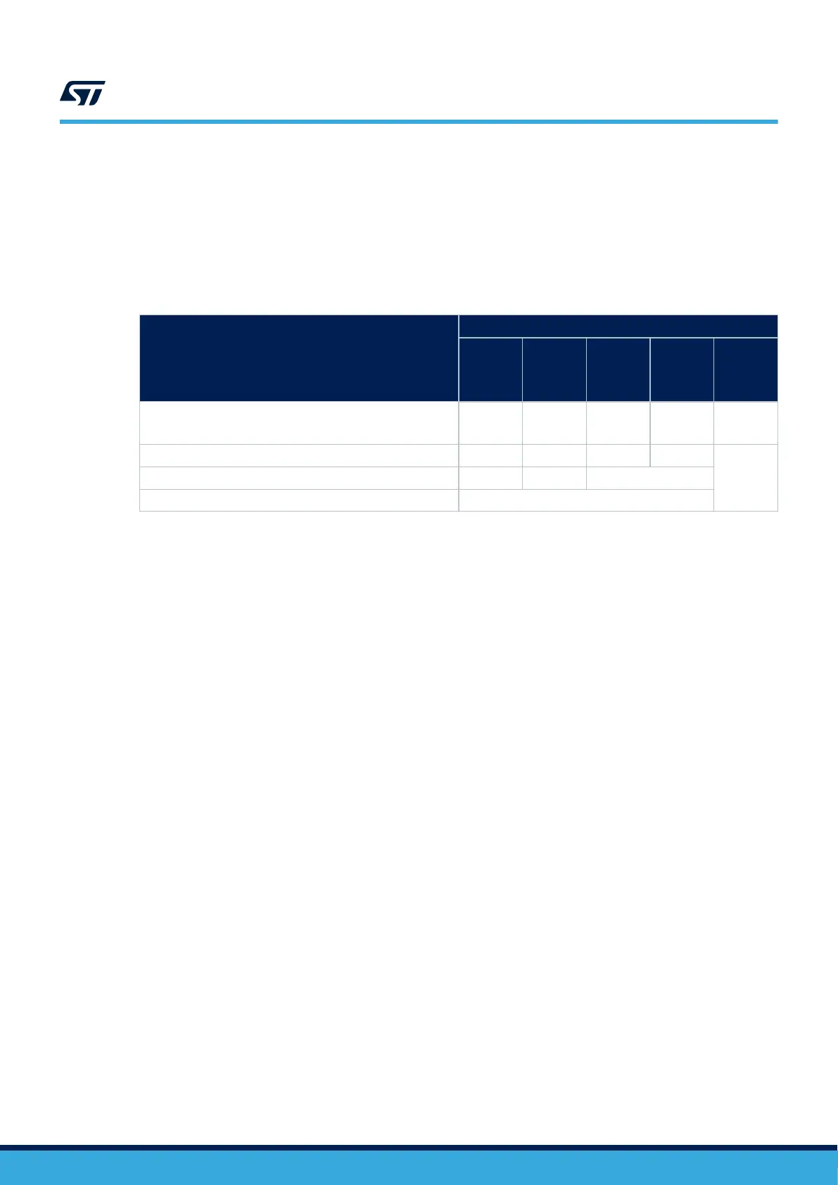
Table 7. SWJ-DP I/O pin availability
Available debug ports
SWJ-DP I/O pin assigned
PA13 /
JTMS/
SWDIO
PA14 /
JTCK/
SWCLK
PA15 /
JTDI
PB3 /
JTDO
PB4/
JNTRST
Full SWJ‑DP (JTAG‑DP + SW‑DP)
Reset state
X X X X X
Full SWJ‑DP (JTAG‑DP + SW‑DP) but without JNTRST X X X X
-JTAG-DP disabled and SW-DP enabled X X -
JTAG-DP disabled and SW-DP disabled Released
6.2.3 Internal pull-up and pull-down resistors on JTAG pins
The JTAG input pins must not be floating since they are directly connected to flip-flops that control the debug
mode features. Special care must be taken with the SWCLK/TCK pin that is directly connected to the clock of
some of these flip-flops.
To avoid any uncontrolled I/O levels, the devices embed the following internal resistors on the JTAG input pins:
• JNTRST: internal pull-up
• JTDI: internal pull-up
• JTMS/SWDIO: internal pull-up
• TCK/SWCLK: internal pull-down
Once a JTAG I/O is released by the user software, the GPIO controller takes the control again, and the software
can then use these I/Os as standard GPIOs. The reset states of the GPIO control registers put the I/Os in the
following equivalent states:
• JNTRST: input pull-up
• JTDI: input pull-up
• JTMS/SWDIO: input pull-up
• JTCK/SWCLK: input pull-down
• JTDO: input floating
Note: The JTAG IEEE standard recommends to add pull-up resistors on TDI, TMS and nTRST, but there is no special
recommendation for TCK. However, for the devices, an integrated pull-down resistor is used for JTCK. Having
embedded pull-up and pull-down resistors removes the need to add external resistors.
AN5373
Pinout and debug port pins
AN5373 - Rev 1
page 23/37
 Loading...


