• The VBAT pin can be connected to an external battery to preserve the content of the Backup domain:
– When VDD is present, the external battery can be charged on VBAT through a 5 kΩ or 1.5 kΩ internal
resistor. In this case, the user can insert a capacitor according to the expected discharging time (1 µF
is recommended).
– If no external battery is used in the application, it is recommended to connect the VBAT pin to V
DD
with
a 100 nF external ceramic decoupling capacitor.
• The VDDUSB pin when present in a package can be connected to a ceramic capacitor of 100 nF.
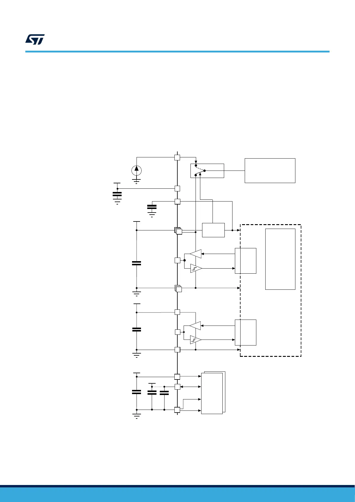
The figures below details the power supply schemes for packages with and without SMPS.
Figure 3. Power supply scheme for STM32U575x and STM32U585x (without SMPS)
V
DDIO2
V
DD
Level shifter
I/O
logic
Kernel logic
(CPU, digital
and
memories)
Backup circuitry
(LSE, RTC, TAMP
backup registers,
backup SRAM)
IN
OUT
LDO
regulator
GPIOs
1.65 – 3.6 V
IN
OUT
GPIOs
n x 100 nF
+ 1 x 10 µF
m x 100 nF
Level shifter
I/O
logic
+ 4.7 µF
m x VDDIO2
m x VSS
n x VSS
n x VDD
VBAT
V
CORE
Power switch
V
DDIO2
V
DDIO1
ADCs/
DACs/
OPAMPs/
COMPs/
VREFBUF
VREF+
VREF-
V
DDA
100 nF
+1 µF
VDDA
VSSA
V
REF
100 nF
+ 1 µF
V
CORE
4.7 µF
VCAP
VDDUSB
3.3 V
100 nF
Caution: If there are two VCAP pins (UFBGA169 package), each pin must be connected to a 2.2 µF (typical) capacitor
(for a total around 4.4 µF).
AN5373
Power supply schemes
AN5373 - Rev 1
page 9/37

 Loading...


