27
Front Panel Interface
The front panel has a 6 phase, multiplexed LED
display and keyboard. U604 is a data bus latch for
U605, a high current driver that provides the strobe
signals to the front panel. Each strobe selects 2
digits and 2 or 3 LED's to be refreshed. Only one
strobe is active at a time. U606 and U609 are pull
down lines for the digits with 390 Ohm current
limiting resistors (N601 and N602). The individual
LEDs are pulled down separately by U613A-
U613C with 12 Ohm current limiting
resistors(R602-R604). They are separated from the
digit pulldowns because the LED's require much
more current than the high efficiency 7 segment
displays. Strobes 2, 3 and 4 also go to the keypad
matrix which is read by U612, an input latch.
U610, a divider chip, takes the system clock of 4
MHz and divides it by 4096 which gives a 977 Hz
signal. This provides the processor with a a real
time interrupt which is used to synchronize
updating the display, analog voltages, and
instrument status.
Low Voltage Power Supplies
(page 7/11)
Line power comes in at the power entry module
where it passes through a fuse and then a RFI filter.
Both the hot and neutral leads are switched. Next,
the voltage passes into the line voltage selector.
The transformer primary is tapped for 4 different
voltages: 100,120, 220, 240 VAC, 50 or 60 Hz.
The transformer has 3 secondaries, 32 VAC non
centertapped and 32 VAC and 15 VAC, center
tapped. The 15 volt tap is rectified by D703 and
D704. It is filtered by C706 to make +8 VDC
unregulated. Then it is regulated by U704 to make
the +5 VDC for the processor, digital logic. U707
regulates the +5VDC for the LED display. The 32
volt tap is full wave rectified by U701 and filtered
by C702 and C705 to provide ±18 VDC. These are
regulated by U702 and U703 to make ±15 VDC for
the analog circuitry.
The 32 volt non center tapped winding is rectified
by D701 and D702, and filtered by C701. It
provides +35 VDC at 1 amp to the pre-regulator for
the high voltage section. U705 provides a regulated
+33 VDC for the control circuits in the pre-
regulator.
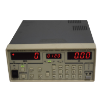
Front Panel
(page 8/11)
The front panel consists of twelve 7 segment high
efficiency displays, a ±1 display, 13 LED's, a
keypad and the high voltage on/off switch.
The displays are multiplexed by 6 strobes. During
each strobe, two of the twelve displays are on. In
addition, up to 2 (of a maximum of 3) LEDs are on
to indicate the instrument status and polarity. The
±1 display is driven the same as the LEDs, but it
has larger current limiting resistors R1 and R2 (390
Ohms), since it is far more efficient then the
ordinary LEDs. Finally strobes 2, 3 and 4 go to the
keypad matrix allowing 1/3 of the keys to be read
during each of these strobe cycles.
The High Voltage ON/OFF switch is separate from
the keypad matrix. Its signals go directly back to
one of the processor's input ports.
High Voltage Section
Note: These boards are covered to prevent
accidental shock or injury. DO NOT ATTEMPT
TO OPERATE THE UNIT WITH THE COVER
OFF !!!
PS310 (page 9/11)
The biggest difference between models in the
PS300 series is the high voltage section. They are
configured to provide the proper combination of
voltage and current through the use of different
diode-capacitor multiplier circuits. For the PS310
(page 9/11), the output of transformer T1 is full
wave rectified by diodes D1-D4 and filtered by C3
and C4. Poles A and B of switch SW1 change the
polarity of the high voltage output and pole C
reports the polarity to the processor. C3, C4 and
R1-R3 are an output filter to reduce switching
noise. R4, R5 and R8 form the divider to provide
the voltage sense signal; R6 and R9 are the current
sense resistor.
PS325 (page 10/11)
The PS325 (page 10/11) is similar to the PS310
except the transformer output is fed to the voltage
doubling circuit of D1, D2, C1 and C2. Switch
SW1 acts in the same fashion as on the PS310.
The voltage sense circuit consists of R4, R5, R6
and R8. R7 and R9 are the current sense resistor.
The output filter is slightly different to reflect the
changes in output voltage and current.