Hardware layout and configuration UM1932
18/30 UM1932 Rev 3
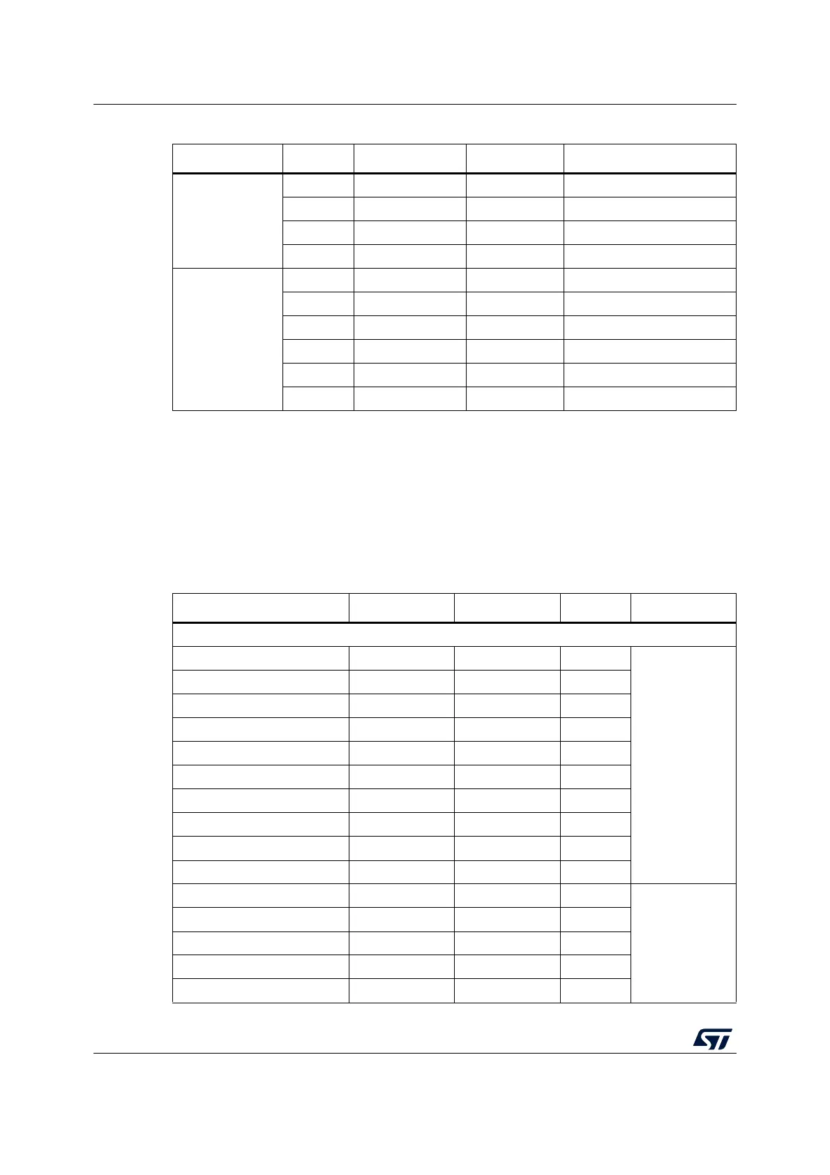
CN6 Power
5 +5V - +5V output
6GND -Ground
7GND -Ground
8 VIN - +6V to +9V power input
(2)
CN8 Analog
1 A0 PB1 ADC12_IN9
2 A1 PC2 ADC12_IN12
3 A2 PC3 ADC12_IN13
4 A3 PC4 ADC12_IN14
5 A4 PC5 or PB9
(3)
ADC12_IN15 or I2C1_SDA
(3)
6 A5 PA4 or PB8
(3)
ADC12_IN4 or I2C1_SCL
(3)
1. Before using pin4 of CN6 as +3.3V input, the solder bridge SB8 must be removed. Otherwise
the board STM32F469I-DISCO could be damaged by the over-current.
2. The external voltage applied to pin VIN must be in the range from 6 V to 9 V at 25°C ambient
temperature. If a higher voltage is applied the regulator U10 may overheat and could be
damaged.
3. By default pin 5 and pin 6 of connector CN8 are PC5 and PA4 respectively. They are enabled
by the default configuration of solder bridges: SB10 and SB12 closed, SB9 and SB11 opened.
If necessary to have an I2C interface on pins 5 and 6 of connector CN8, change the
configuration solder bridges: open SB10 and SB12, close SB9 and SB11.
Table 5. ARDUINO
®
compatible connectors
Function MCU Pin Pin name Pin Connector
RIGHT connectors
I2C1_SCL PB8 D15 10
CN5 Digital
I2C1_SDA PB9 D14 9
AVDD - AVDD 8
Ground - GND 7
SPI2_SCK PD3 D13 6
SPI2_MISO PB14 D12 5
TIM12_CH2, SPI2_MOSI PB15 D11 4
TIM12_CH1, SPI2_CS PH6 D10 3
TIM14_CH1 PA7 D9 2
-PG10D81
-PG11D78
CN7 Digital
TIM3_CH1 PA6 D6 7
TIM5_CH3 PA2 D5 6
-PG12D45
TIM5_CH2 PA1 D3 4
Table 4. ARDUINO
®
compatible connectors (continued)
Connector Pin Pin name MCU Pin Function