Chapter 2: Installation
2-33
J5
T-SGPIO2
T-SGPIO1
JLAN2
JLAN1
JF1
1
COM2
JWOL
Battery
JSM1
JSM2
JBT1
JUSB3
1
BMC/VGA
CTRL
J26
JPG1
JPL1
JPL2
JWD
JPS1
JPT1
JI2C2
JI2C1
D1
LE1
LES2
J6
JD1
SP1
JOH1
JL1
JPS2
JPW3
JPW1
JPW2
1
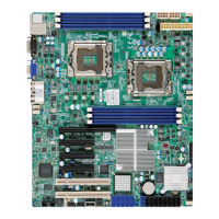
X8DT3/i Series
BIOS
LAN3
LAN1
LAN2
VGA
Slot6 PCI-E 2.0x8
PCI 33 MHz
I-BUTTON
P1-DIMM3A
P1-DIMM3B
P1-DIMM2A
P1-DIMM2B
P1-DIMM1A
P1-DIMM1B
P2-DIMM1A
P2-DIMM2B
P2-DIMM2A
P2-DIMM3B
SAS4~7
SAS0~3
Fan6
Fan5
Fan2
Fan8/
CPU2 FAN
Fan4
Fan3
Fan7/
CPU1
Fan1
Slot3
P2-DIMM3A
KB/MOUSE
COM1
LAN4
Slot2 PCI-E x4
-
I-SATA1
-
I-SATA3
-
Slot1 PCI 33MHz
Floppy
USB6/7
USB4/5
USB3
USB2
USB 0/1
I-SATA5
P2-DIMM1B
LAN
CTRL
LAN
CTRL
Slot5 PCI-E 2.0x8 in x16
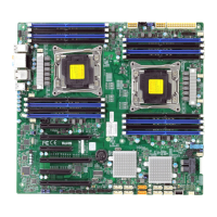
CPU2
CPU1
ICH10R
North Bridge
LSI
1068E
LES1
(X8DT3/i-LN4F)
SI/O
(*X8DT3 Models only)
SPEC
Dedicated LAN
Slot4 PCI-E 2.0 x16
(X8DT3/i-F/-LN4F only)
(*X8DT3 Models only)
J27J28
JPB
Intel 5520
South Bridge
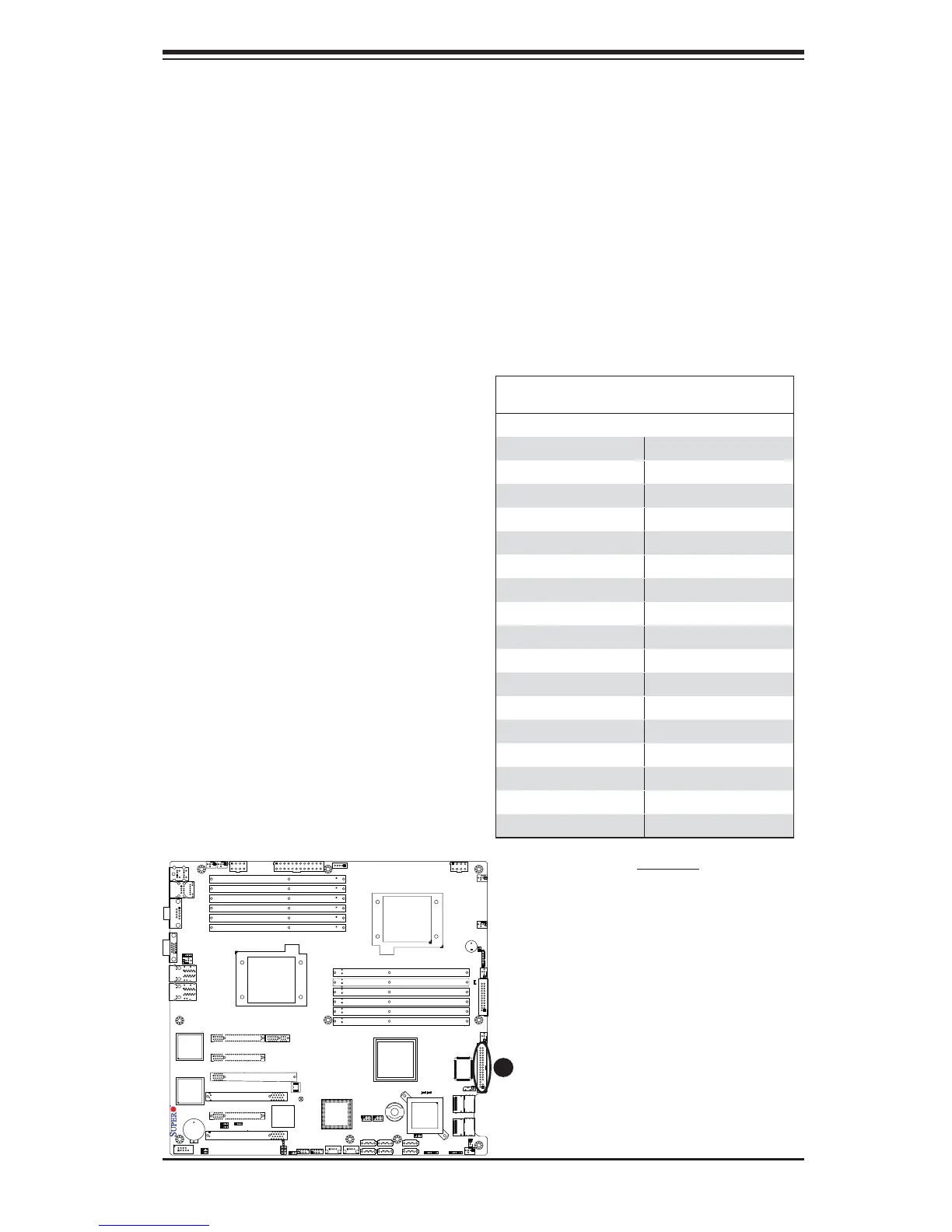
Floppy Connector
The fl oppy connector is located next
to the Super I/O chip on the mother-
board. See the table on the right for
pin defi nitions.
Floppy Drive Connector
Pin Defi nitions
Pin# Defi nition Pin # Defi nition
1 Ground 2 FDHDIN
3 Ground 4 Reserved
5 Key 6 FDEDIN
7 Ground 8 Index
9 Ground 10 Motor Enable
11 Ground 12 Drive Select B
13 Ground 14 Drive Select B
15 Ground 16 Motor Enable
17 Ground 18 DIR
19 Ground 20 STEP
21 Ground 22 Write Data
23 Ground 24 Write Gate
25 Ground 26 Track 00
27 Ground 28 Write Protect
29 Ground 30 Read Data
31 Ground 32 Side 1 Select
33 Ground 34 Diskette
A
A. Floppy
2-9 Floppy Drive, Serial ATA and SAS Connections
Note the following when connecting the fl oppy and hard disk drive cables:
The fl oppy disk drive cable has seven twisted wires.
•
A red mark on a wire typically designates the location of pin 1.•
A single fl oppy disk drive ribbon cable has 34 wires and two connectors to •
provide for two fl oppy disk drives. The connector with twisted wires always
connects to drive A, and the connector that does not have twisted wires always
connects to drive B.
 Loading...