Chapter 2: Installation
2-27
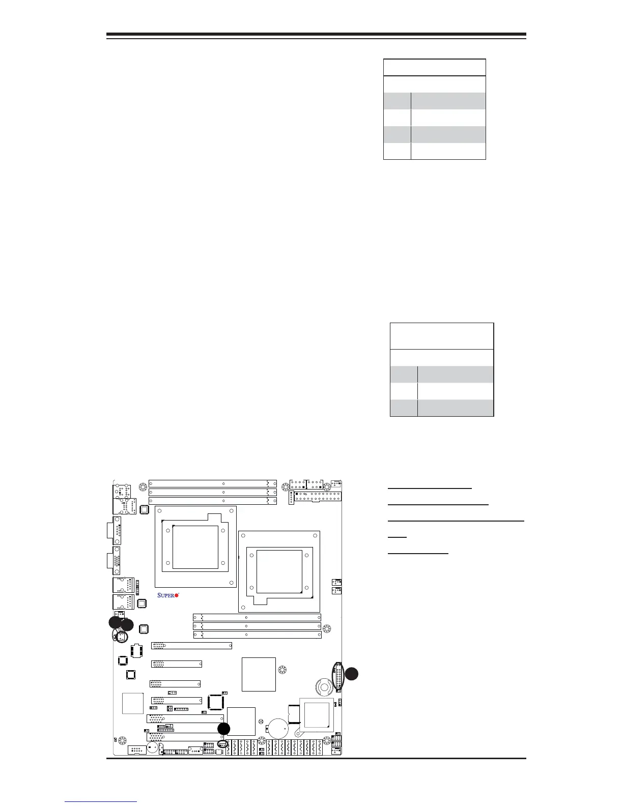
JPW3
JPW2
JBT1
JPI2C
COM1
I-SATA0
I-Button
JPS1
JWD
JPL2
JPL1
JF1
SP1
JWOL
LE1
D20
JBAT1
JP3
JL1
JPS2
JOH1
JPB
JP5
J16
JD1
CPU1 FAN
Slot3 PCI-E 1.0 x4
7HG
5ADG
7TN100C
W8379
W8352
Slot6 PCI-E 2.0 x8 (in x16 Slot)
JI2C2
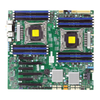
SAS6
SAS5
SAS4
SAS3
SAS2
SAS1
Slot4 PCI-E 2.0 x8
BMC CTRL
WPCM450-R
LC4128ZE-
ICH10R
(South Bridge)
5500
(North Bridge)
LES2
P1-DIMM3A
P1-DIMM1A
P2-DIMM3A
P1-DIMM2A
P2-DIMM2A
P2-DIMM1A
KB/Mouse
USB0/1
VGA
LAN1
UID
LE2
Slot2 PCI 33MHz
Slot1 PCI 33MHz
COM2
IPMB
USB4/5
USB6
T-SGPIO2
USB2/3
I-SATA5
T-SGPIO1
I-SATA3
I-SATA2
I-SATA4
I-SATA1
3-SGPIO2
3-SGPIO1
LSI SAS1068E
SAS0
FAN5
FAN4
FAN6
FAN1/
CPU2
LAN2
IPMI LAN
LAN
CTRL
SAS7
JI2C1
LAN
CTRL
PHY
Chip
CPU1
Intel
Intel
JPW1
CPU2FAN
FAN2/
BIOS
Slot5 PCI-E 2.0 x4 (in x8 Slot)
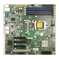
X8DTL Series
Flash ROM
BMC
Battery
Buzzer
1
FAN3
JPG1
(in x8 Slot)
Rev. 2.01
JWOR
JWF1
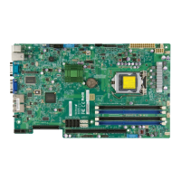
A
B
A. Rear UID Switch
B. Rear UID LED (LE2)
C. Front UID LED (Pin 7 of
JF1)
D. DOM PWR
Unit Identifi cation Switch/LEDs
There are three Unit Identifi cation (UID) de-
vices on the motherboard. A rear UID switch
and a rear UID LED indicator are located
next to Fan 6 on the back of the chassis.
The Front Panel UID LED is connected to a
pin in the Front Control Panel (Pin 7 of JF1).
When the user pushes the rear UID switch,
the Front Panel UID LED and the backplane
UID LED (LE2) will be turned on. Push the
rear UID switch again to turn off both Indi-
cators. These UID Indicators provide easy
identifi cation of a system unit that may be in
need of service.
UID Switch
Pin# Defi nition
1 Ground
2 Ground
3 Button In
4 Ground
C
DOM Power Connector
A power connector for the SATA DOM (Disk_
On_Module) devices is located at JWF1.
Connect an appropriate cable here to provide
power support for your DOM devices. (This
connector is available on the PCB R2.01 or
a later version board only.)
DOM PWR
Pin Defi nitions
Pin# Defi nition
1 +5V
2 Ground
3 Ground
 Loading...