TB9100 Reciter Service Manual Appendices 127
© Tait Electronics Limited January 2006
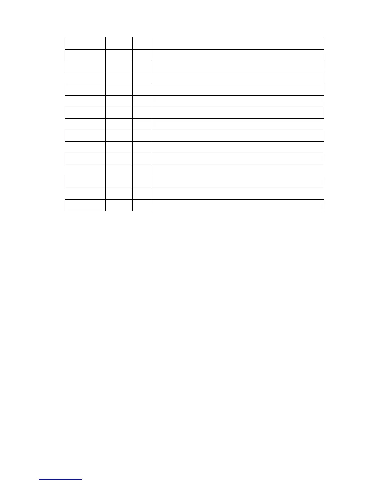
SDRAS A11 O/P SDRAM row address strobe
SDWE B12 0/P SDRAM write enable
SSADS N4 O/P SBSRAM address strobe
SSOE M3 O/P SBSRAM output enable
SSWE M2 O/P SBSRAM write enable
TCK L17 I/P IEEE Standard 1149.1 test clock
TDI L16 I/P IEEE Standard 1149.1 test data input
TDO L16 O/P IEEE Standard 1149.1 test data output
TIN/TOUT0 P15 I/O Timer 0 input/output
TIN/TOUT1 R17 I/O Timer 1 input/output
TMS K14 I/P IEEE Standard 1149.1 test mode select
TRST C17 I/P IEEE Standard 1149.1 test reset
VSS PWR Ground
XF B2 O/P External flag output
Table 8.11 TMS320VC5510 Port Assignments (Continued)
Pin Name Pin No. Type Function

 Loading...


