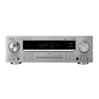
Do you have a question about the Teac AG-D9260 and is the answer not in the manual?
Details output power, input sensitivity, frequency response, and signal-to-noise ratios for audio amplification.
Specifies sampling frequencies and digital input levels/impedances for audio processing.
Lists tuning range, sensitivity, distortion, and signal-to-noise ratios for FM reception.
Details tuning range, sensitivity, distortion, and signal-to-noise ratios for AM reception.
Outlines input and output sensitivity and impedance for video signals.
Covers power requirements, consumption, dimensions, weight, and included accessories.
Guidelines for safe servicing, part replacement, and internal wiring integrity.
Instructions on handling mechanical parts, preventing static discharge, and laser safety.
Guidance on the proper disposal of batteries to protect the environment.
Procedures for leakage current and resistance measurements post-repair.
Lists required equipment and important parameters for system alignment.
Identifies specific points on the circuit board for calibration adjustments.
Calibrating FM and AM tuning frequency ranges using a DC voltmeter.
Adjusting AM tracking for maximum sensitivity using a signal generator.
Calibrating FM RF circuits for maximum sensitivity via signal generator.
Adjusting FM mono distortion levels using a DC voltmeter.
Setting the auto stop level thresholds for FM and AM tuning.
Diagram illustrating the FIP display segments and their functions.
Table mapping FIP display pins to their respective anode connections.
Visual representation of the main connector's pin arrangement.
Detailed mapping of pin numbers to their specific functions or signals.
Detailed pin functions and descriptions for the U-COM microcontroller (IC71).
Listing of pin numbers and their corresponding functions for the microcomputer.
Internal functional blocks and data flow of the microcomputer IC.
Detailed pin functions and descriptions for the DTS decoder IC (YSS912C).
Comprehensive table of pin functions and descriptions for YSS912C.
Visual representation of the YSS912C integrated circuit's pinout.
Block diagram illustrating the internal structure and interfaces of the YSS912C.
Internal architecture and signal paths of the electronic volume/input IC.
Internal architecture and signal paths of the ADC/DAC/input IC.
Pin configuration and assignment for the 74HCU04AFN hex inverter IC.
Graphical symbol and operational truth table for the hex inverter.
Internal structure of the AK4112AVF digital input IC for serial and parallel modes.
Internal structure of the PLL synthesizer/tuner IC (LC72131).
Internal structure of the MPX + IF/tuner IC (LA1837).
Internal architecture of the KIC9164AF function/input IC.
Internal architecture of the KIC9163AF function/input IC.
Internal structure of the NJM2296M main IC (multiplexer).
Pin functions and configuration for the LA6462M/6458M multiplex IC.
Block diagrams for various transistors and regulator ICs.
Block diagram for the LA7952 video switch/input IC.
Visual representation of the unit's components and their assembly order.
List of numbered parts with corresponding part numbers and quantities.
Detailed list of parts, their numbers, and descriptions for various assemblies.
List of fuses, cables, and other accessory items included with the unit.
Diagram illustrating the placement of components on the main printed circuit board.
Diagrams showing component placement on various secondary circuit boards.
Illustrations of component placement on diverse printed circuit boards.
List of components and part numbers for the input PCB assembly.
List of components and part numbers for the front PCB assembly.
Detailed list of components and their part numbers for the main PCB.
List of accessories provided with the unit, including manuals and antennas.
The primary circuit diagram illustrating the complete system architecture.
Further schematic diagrams detailing specific functional blocks of the receiver.
Final schematic diagrams covering various sections of the unit.
Guidelines for service technicians on safety checks and measurements.
| Power Output | 100W per channel (8 ohms, 20Hz-20kHz, 0.08% THD) |
|---|---|
| Total Harmonic Distortion (THD) | 0.08% |
| Input Impedance | 47k ohms |
| Input sensitivity | 200mV (line) |
| Signal-to-Noise Ratio | 100dB |
| Dimensions | 435 x 170 x 422 mm |
| Tuning range | FM |
| Speaker load impedance | 8 ohms |
| Video Connections | Composite Video |