Do you have a question about the Technics SA-EH670 and is the answer not in the manual?
Details amplifier power output, distortion, and load impedance.
AM/FM tuner frequency range, sensitivity, and S/N ratios.
Clock, timer functions, and general unit specifications.
Procedures for safe power handling and initial voltage check before operation.
Steps to diagnose and resolve protection circuit issues like no sound.
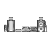
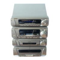
List of components and accessories supplied with the main unit.
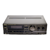
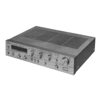
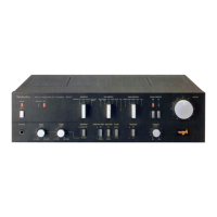
Identification of front panel controls, buttons, jacks, and indicators.
Procedure to check and inspect the AC IN printed circuit board.
Procedure to check and inspect the main operation printed circuit board.
Procedure to check and inspect the main printed circuit board.
Procedure for safely replacing the regulator transistor.
Procedure for safely replacing the power IC.
Method to supply power to the unit for testing without a system.
How the unit displays malfunction codes for diagnosis and service.
Steps to exit diagnostic mode and restore normal operation.
Explains malfunction codes and common communication errors.
Explains switch nomenclature, VR901, and important safety notices.
Important safety notices and handling precautions for components like ICs.
Lists IC terminal functions, focusing on System Control/FL Drive.
Visual representations of ICs, transistors, diodes, and their markings.
Diagram showing how different PCBs connect to each other.
High-level block diagram of the system and key IC connections.
Block diagram illustrating the power supply regulation stages.
Explains safety notices, language marks, and retention time indicators.
Visual guide to the location of cabinet parts and components.
Illustrations and notes regarding the packaging of the unit.
Detailed layout of the Main Printed Circuit Board.
Layouts for the AC IN and Power Transformer PCBs.
Layouts for the Operation and Power Supply PCBs.
Schematic of the unit's main operation circuit.
Schematic for the system control and FL drive functions.
Schematic for the RDS signal demodulator circuit.
Schematic detailing the main circuit connections and components.
Schematic of the power amplifier section.
Schematic of the power supply circuit and regulators.
Schematics for AC input and power transformer circuits.
Schematic of the tuner unit, including PLL synthesizer.
Schematic for IF amplifier, control, and switching circuits.
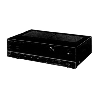
Identifies front panel buttons and jacks on the main unit.
Explains the buttons and functions of the remote control.
| Type | Stereo Receiver |
|---|---|
| Power Output | 100 W |
| Impedance | 8 Ohms |
| Total Harmonic Distortion (THD) | 0.08% |
| Total Harmonic Distortion | 0.08% |
| Frequency Response | 20 Hz - 20 kHz |
| Input Sensitivity | 200 mV |
| Signal-to-Noise Ratio | 80 dB |
| Speaker Impedance | 8 Ohms |
| Dimensions | 430 x 150 x 320 mm |
| Weight | 8 kg |
| Speaker load impedance | 8 ohms |
| Video inputs | composite |