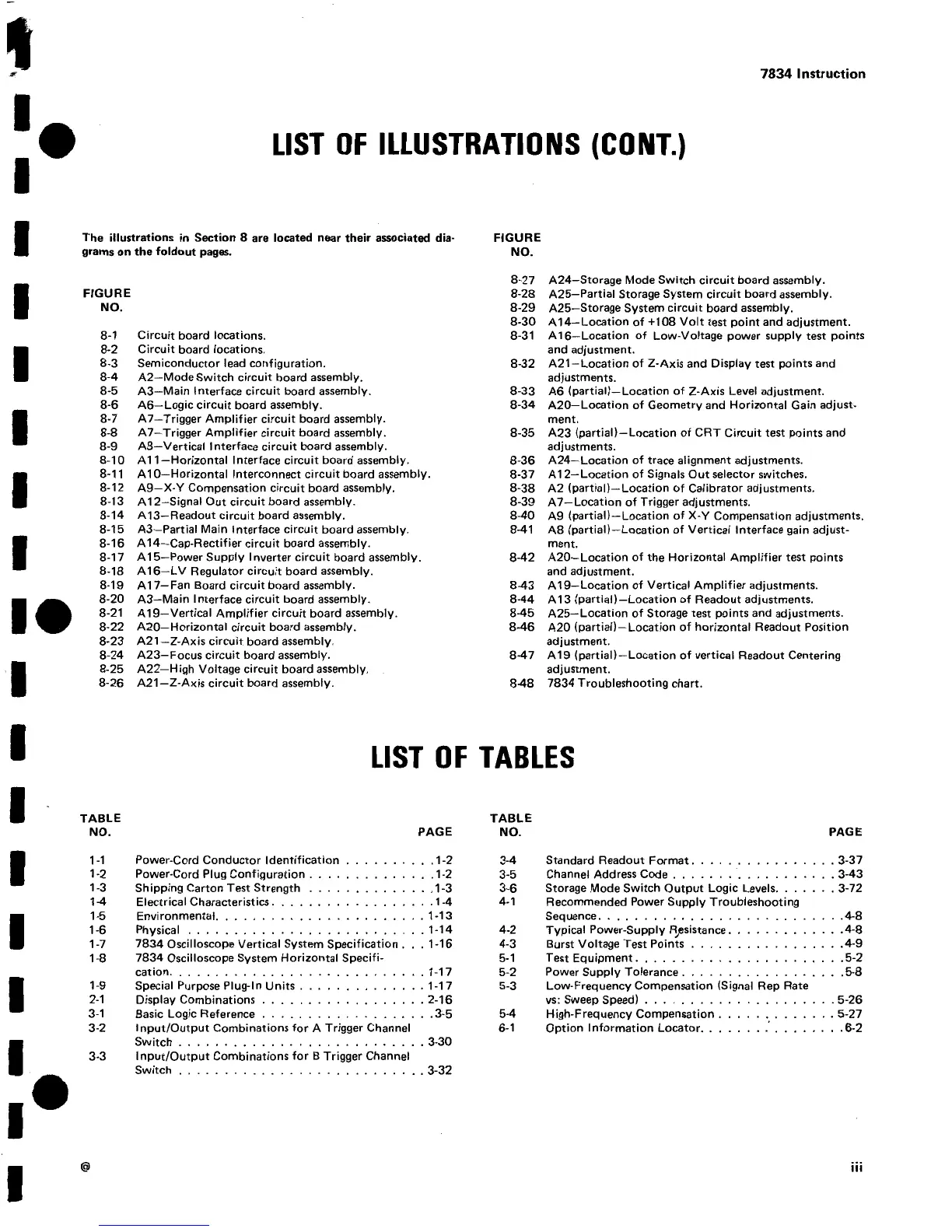
LIST
OF
ILLUSTRATIONS
(CONT
.)
LIST
OF
TABLES
7834
Instruction
TABLE
NO
.
PAGE
TABLE
NO
.
PAGE
1-1
Power-Cord
Conductor
Identification
. . . . . . . . .
.1-2
3-4
Standard
Readout
Format
. . . . . . . .
.
. . . .
.
3-37
1-2
Power-Cord
Plug
Configuration
. . . . . . . . . . . . .
.1-2
3-5
Channel Address
Code
. .. . . . . . . . . . . . . . .
.
3-43
1-3
Shipping
Carton
Test
Strength
. . . . . . . . . . . . .
.1-3
3-6
Storage
Mode
Switch
Output
Logic
Levels
. . . . . .
.
3-72
1-4
Electrical
Characteristics
.
.1-4
. . . . . . . . . . . . . . .
.
4-1
Recommended
Power
Supply
Troubleshooting
1-5
Environmental
. . . .
. . .
1-13
. . . . . . . . . . . . . . . .
Sequence
.
. . . . . .
. . .
. . . . . . . . . . . . . .
. .
.48
1-6
Physical
. . . . .
.1-14
.
. . .
. . .
. . .
. .
.
. . . . . . .
4-2
Typical
Power-Supply
Resistance
. . . . . . . . . . . .
.4-8
1-7
7834
Oscilloscope
Vertical
System
Specification
. . .
1-16
4-3
Burst
Voltage
Test
Points
. . . . . . . . . . . . . . . .
.4-9
1-8
7834
Oscilloscope
System
Horizontal
Specifi-
5-1
Test
Equipment
. . . . . . . . . . . . . . . . . . . . . .
.5-2
cation
.
. .
.
.
. . . .
. .
.
.
.
1-17
. . . . . . . .
.
.
.
. .
.
5-2
Power Supply
Tolerance
. . . . . . . . . . . . . . . . .
.5-8
1-9
Special
Purpose
Plug-In
Units
1-17
. . . . . . . . . . . . . .
5-3
Low-Frequency
Compensation
(Signal
Rep
Rate
2-1
Display
Combinations
2-16
. . . . . . . . . . . . . . . . . .
vs
:
Sweep
Speed)
.
. . .
.
. .
.
. . . . .
. . .
. . . .
.
5-26
3-1
Basic Logic
Reference
. . . . . . . . . . . . . . . . .
.
.3-5
5-4
High-Frequency
Compensation
. . . . .
. .
.
.
.
. .
5-27
3-2
Input/Output
Combinations
for
A
Trigger
Channel
6-1
Option
Information
Locator
. . . .
.
. . . . . .
.
.
. .
.6-2
Switch
. . . . . . . . . . . .
3-30
. . . . . . . . . . . .
. . .
3-3
Input/Output
Combinations
for
B
Trigger
Channel
Switch
. . . . . . .
3-32
. . . . . . . . . . . . . . .
. . . . .
The
illustrations
in
Section
8
are
located
near
their
associated
dia-
FIGURE
grams on
the
foldout
pages
.
NO
.
8-27
A24-Storage
Mode
Switch
circuit
board
assembly
.
FIGURE
8-28
A25-Partial
Storage
System
circuit
board
assembly
.
NO
.
8-29
A25-Storage
System
circuit
board
assembly
.
8-30
A14-Location
of
+108
Volt
test
point
and
adjustment
.
8-1
Circuit
board
locations
.
8-31
A16-Location
of
Low-Voltage
power
supply
test
points
8-2
Circuit
board
locations
.
and
adjustment
.
8-3
Semiconductor
lead
configuration
.
8-32
A21-Location
of
Z-Axis
and
Display
test
points
and
8-4
A2-Mode
Switch
circuit
board
assembly
.
adjustments
.
8-5
A3-Main
Interface
circuit
board
assembly
.
8-33
A6
(partial)
-Location
of
Z-Axis
Level
adjustment
.
8-6
A6-Logic
circuit
board
assembly
.
8-34
A20-Location
of
Geometry
and
Horizontal
Gain
adjust-
8-7
A7-Trigger
Amplifier
circuit
board
assembly
.
ment
.
8-8
A7-Trigger
Amplifier
circuit
board
assembly
.
8-35
A23
(partial)-Location
of
CRT
Circuit
test
points
and
8-9
A8-Vertical
Interface
circuit
board
assembly
.
adjustments
.
8-10
A11-Horizontal
Interface
circuit
board
assembly
.
8-36
A24-Location
of
trace
alignment
adjustments
.
8-11
A10-Horizontal
interconnect
circuit
board
assembly
.
8-37
Al
2-Location
of
Signals
Out
selector
switches
.
8-12
A9-X-Y
Compensation
circuit
board
assembly
.
8-38
A2
(partial)-Location
of
Calibrator
adjustments
.
8-13
A12-Signal
Out
circuit
board
assembly
.
8-39
A7-Location
of
Trigger
adjustments
.
8-14
A13-Readout
circuit
board
assembly
.
8-40
A9
(partial)-Location
of
X-Y
Compensation
adjustments
.
8-15
A3-Partial
Main
Interface
circuit
board
assembly
.
8-41
A8
(partial)-Location
of
Vertical
Interface
gain
adjust-
8-16
A14-Cap-Rectifier
circuit
board
assembly
.
ment
.
8-17
A15-Power
Supply
Inverter
circuit
board
assembly
.
8-42
A20-Location
of
the
Horizontal
Amplifier
test
points
8-18
A16-LV
Regulator
circuit
board
assembly
.
and
adjustment
.
8-19
A17-Fan
Board
circuit
board
assembly
.
8-43
A19-Location
of
Vertical
Amplifier
adjustments
.
8-20
A3-Main
Interface
circuit
board
assembly
.
8-44
A13
(partial)
-Location
of
Readout
adjustments
.
8-21
A19-Vertical
Amplifier
circuit
board
assembly
.
8-45
A25-Location
of
Storage
test
points
and
adjustments
.
8-22
A20-Horizontal
circuit
board
assembly
.
8-46
A20
(partial)
-Location
of horizontal
Readout
Position
8-23
A21
-Z-Axis
circuit
board
assembly
.
adjustment
.
8-24
A23-Focus
circuit
board
assembly
.
8-47
A19
(partial)
-Location
of
vertical
Readout
Centering
8-25
A22-High
Voltage
circuit
board
assembly
.
adjustment
.
8-26
A21-Z-Axis
circuit
board
assembly
.
8-48
7834
Troubleshooting
chart
.