Theory of Operation-AA
501
Automatic Gain Control
0
The output of the input amplifier feeds the agc circuitry at
levels between 0.75 V and 3.0 V for inputs greater than
50
mV, and the agc automatically adjusts the signal to a
constant 2
Vac. This is the reference level for the subse-
quent distortion measuring circuits.
The
agc circuitry is composed of attenuator R1431,
U1331, U1431, R1432, and amplifier U1430. The control
element in the
agc is a pair of light-dependent resistors
(LDR's), U1331 and U1431. Thesedevicesconsist of alight
emitting diode and a semiconductor resistance cell in one
package. As more control current is forced through the
LED'S, the cells are illuminated more brightly and their
cell's resistance decreases. This shunts more signal to
ground. Two LDRs are used in series with shunting
resistors
R1338 and R1339 to minimize distortion at the
signal levels present.
The control circuitry for the
agc consists of active rectifi-
er,
U1330B with diodes CR1332 and CR1333. The filters
are composed of
U1530A and U1530B and associated com-
ponents. The circuitry seeks to keep the voltage at the out-
put pin
6
of low noise operational amplifier U1430 at about
2.0 V. This output voltage is varied to standardize the THD
measurements by adjusting
R1330, the DlST CAL control.
'The output of U1430 is fullwave rectified by U1330B with
diodes
CR1332, CR1333 and integrated by U1530A and
C1533 with the reference current from R1330. Amplifier
U1530B in conjunction with C1530, C1534, R1530 and
R1531 provides additional filtering of the rectified voltage to
reduce distortion introduced by the
agc action. Transistor
Q1530 provides the current drive necessary for the LDRs,
while VR1430 linearizes the open loop gain of the agc loop
to optimize transient response at all signal amplitudes.
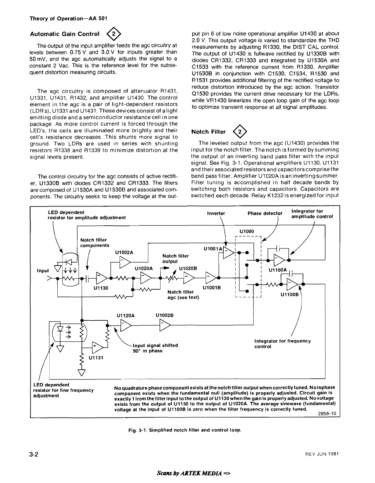
Notch Filter
@
The leveled output from the agc (U1430) provides the
input for the notch filter. The notch is formed by summing
the output of an inverting band pass filter with the input
signal. See Fig.
3-1. Operational amplifiers U1130, U1131
and their associated resistors and capacitors comprise t he
band pass filter. Amplifier
U1020A isaninvertingsummer.
Filter tuning is accomplished in half decade bands by
switching both resistors and capacitors. Capacitors are
switched each decade. Relay
K1232 is energized for input
LED dependent Inverter Phase detector Integrator
'Or
amplitude control
Notch filter
Notch filter
agc (see text)
I
control
Integrator for frequency
Input signal shifted
90' in phase
LED
dependent
resistor for fine frequency
No quadrature phase component exists at the notch filter output when correctly tuned. No
inphase
adjustment
component exists when the fundamental null (amplitude) is properly adjusted. Circuit gain is
exactly 1 from the filter input
tothe output of U1130 when the gain is properly adjusted. Novoltage
exists from the output of
U1130 to the output of U1020A. The average sinewave (fundamental)
voltage at the input of
UllOOB is zero when the filter frequency is correctly tuned.
2958-
10
Fig. 3-1. Simplified notch filter and control loop.
REV
JUN
1981
Scans
by
ARTEK
MEDLA
=>