TCC8900 TCC8900_DEMO_AM_2747_V1.1 July, 31, 2009
Board Guide TCC8900 DEMO BOARD PIN DESCRIPTION
Preliminary 1-6
z Other Pins of Main Board
-JP46: SDMMC_MS_SEL
-JP48: CAS_PWR_SEL
-JP51: BT_PWR_SEL
-JC1: RCA Connector
-JC2: Head Phone Connector
-JC3: Line in Connector
-JS6: JTAG_OE
z Boot Mode CS Pin
-JS1:BM2 Boot Mode 2 bit setting jumper (refer to TCC8900 datasheet)
-JS2:BM1 Boot Mode 1 bit setting jumper (refer to TCC8900 datasheet)
-JS3:BM0 Boot Mode 0 bit setting jumper (refer to TCC8900 datasheet)
-JS4:UTXD1 Boot Mode Sub 1 bit setting jumper (refer to TCC8900 datasheet)
-JS5:UTXD0 Boot Mode Sub 0 bit setting jumper (refer to TCC8900 datasheet)
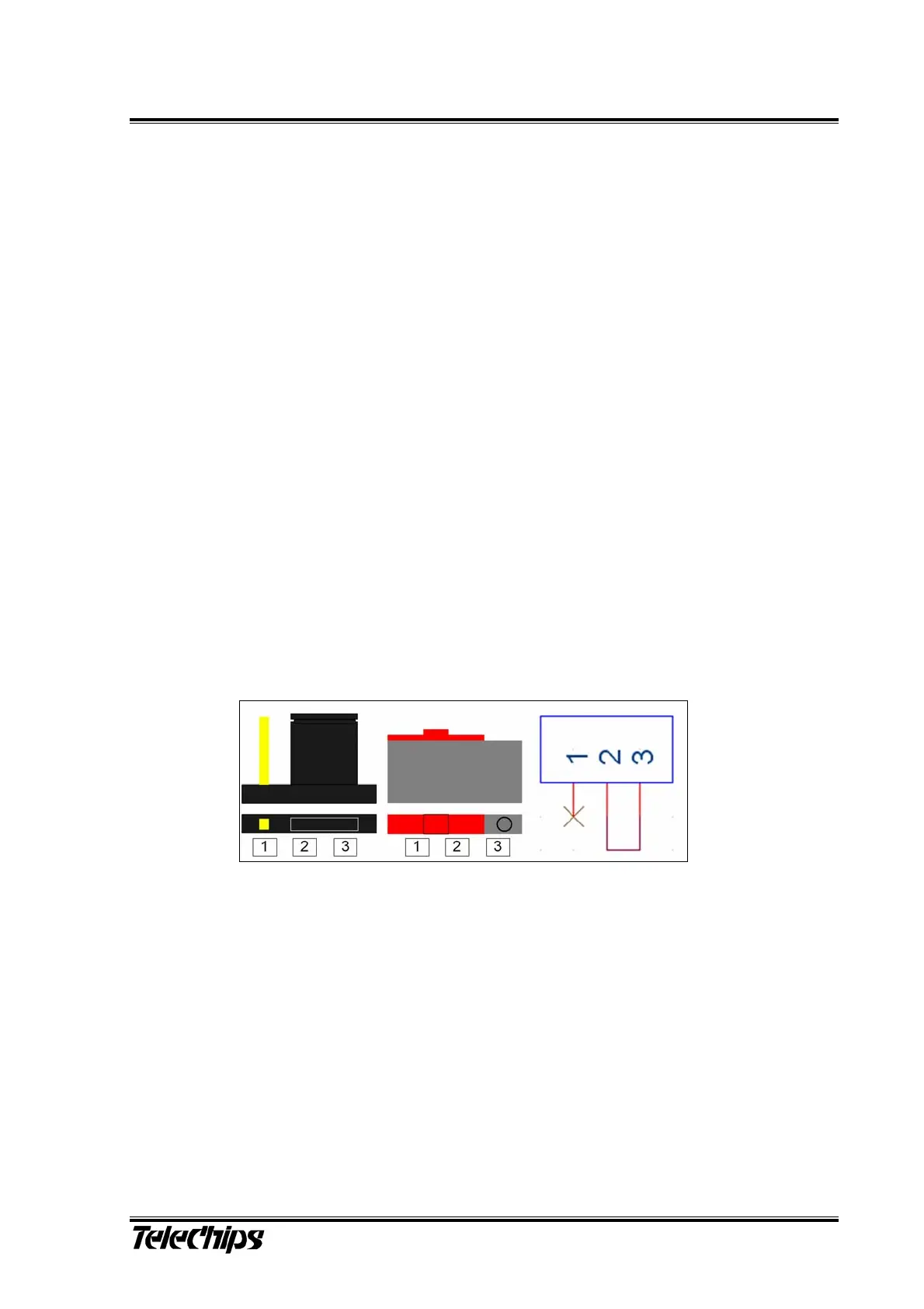
JS1 ~ JS7
1-2: logical ‘High’ Switch Down
2-3: logical ‘Low’ Switch Up
Cover the jumper cap to connect pin#2 and pin#3 as can be seen in the picture below.
In opposition to jumper cap-mounting, if the slide of slide switch is pushed to the left,
the middle and the right pins are connected to each other.
Note the circles on pin #1 and pin # 3 of the slide switch.
Figure 5. Jumper Cap Connection