GE910 Hardware User Guide
1vv0300962 Rev.12 2013-10-22
Reproduction forbidden without Telit Communications S.p.A. written authorization - All Rights Reserved
page 67 of 83
Mod. 0805 2011-07 Rev.2
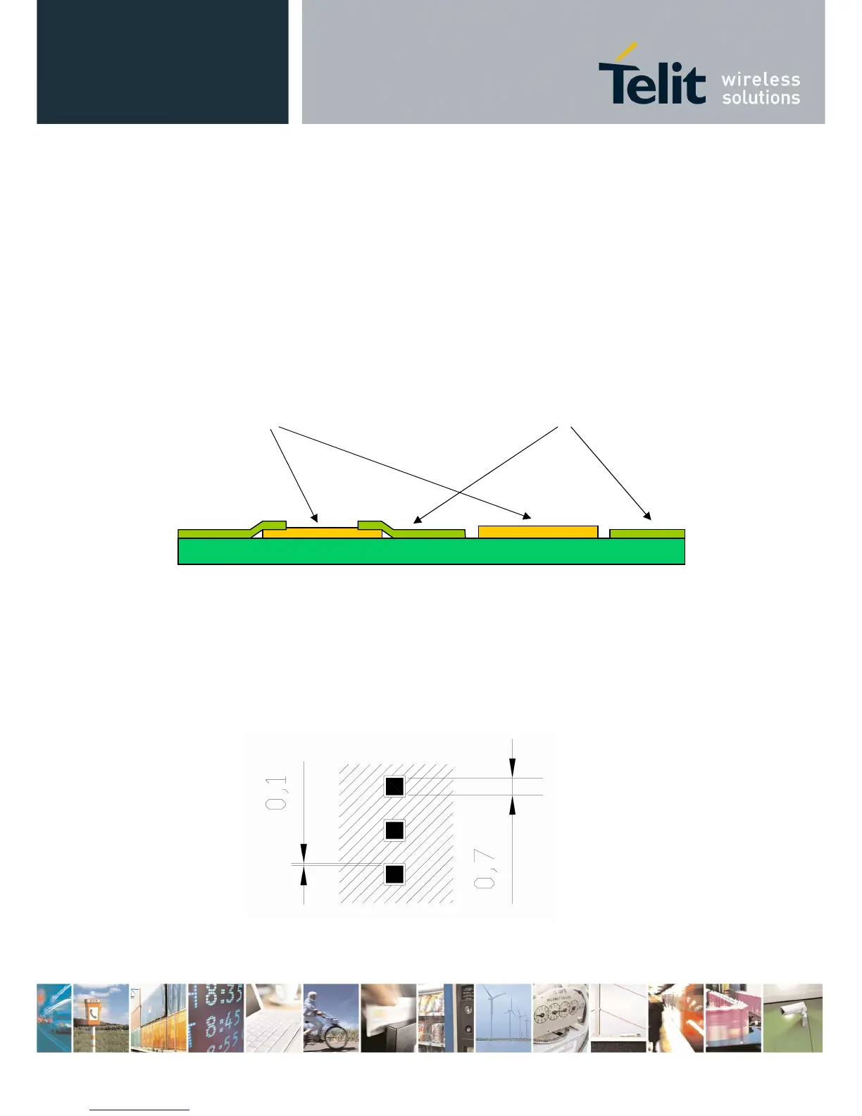
13.4. Stencil
Stencil’s apertures layout can be the same of the recommended footprint (1:1), we suggest a
thickness of stencil foil 120µm.
13.5. PCB pad design
Non solder mask defined (NSMD) type is recommended for the solder pads on the PCB.
13.6. Recommendations for PCB pad dimensions
Units are in mm.
PCB